LED semiconductor lighting network information For switching power supplies, safety and reliability have always been regarded as one of the important performance. The switching power supply can work safely and reliably under the condition that the electrical technical specifications meet the requirements of normal use of electronic equipment, and also meet the external or own circuit or load circuit failure. Therefore, various protection measures are required. Analysis of the characteristics of the protection circuit, and the lack of expectation to overcome, hope to design a safer and more reliable protection circuit.
1. Analysis of surge current circuit
The inrush current is caused by a sudden change in voltage. For example, when the electronic device is applied with voltage for the first time, the initial current is injected due to the charging of the large-capacity power supply capacitor. The surge current is turned on; and the sudden change of the lightning strike and the induced lightning enters the switching power supply along the power line. The transient current generated by the voltage is the lightning surge current. The surge current rises very quickly, the duration is very short, and the damage is very large. In order to prevent or reduce the damage of the inrush current, set the way to suppress the inrush current or transfer the inrush current to the ground to protect the switching power supply from the inrush current.
1.1 Start current limiting protection
The primary rectifying circuit of the switching power supply has a large-capacity filter capacitor, and the rectifier tube charges the large capacitors at the instant of starting, so that the instantaneous current of the rectifier exceeds the rated value. In order to reduce the starting current limit (surge current), switching power supplies are usually equipped with anti-shock circuits. As shown in the circuit of Figure 1, at the instant of power-on, the voltage of the 3 and 4 windings of the switching power supply transformer is 0V, VD5 is cut off, and the voltage between the G and K poles of the thyristor VD6 is 0V, and VD6 is cut off. Charging current path: AC220V→VD1- 4 positive → large capacitance C1 → ground → R2 → VD1 4 negative. Since R2 has a large current blocking effect (generally set to 3.3 Ω??), it can effectively limit the starting surge current.
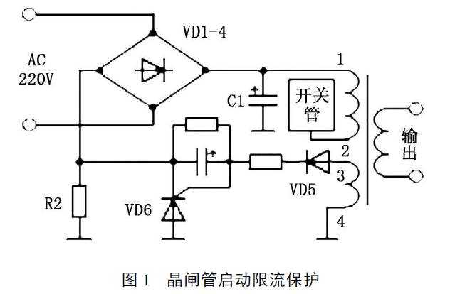
After the switching power supply works normally, the induced voltage is generated on the 1 and 2 windings of the switching power supply transformer, and C2 is charged (the charging time constant is approximately equal to R3×C2), so that VD6 is turned on, the rectified current is no longer passed through R2, but is passed through VD6. A, K pole return to the negative pole of rectifier bridge VD1 - 4. In other words, in normal operation, VD6 shorts R2 to prevent R2 from generating power. R2 only works at the moment of power on.
The use of thyristor as the starting current limiting protection is safe and reliable, but the circuit is more complicated. From the perspective of circuit cost and simple circuit, the temperature-controlled resistor is used for starting current limiting protection, which is economical, simple, safer and more reliable, as shown in Fig. 3.
1.2 lightning surge current protection
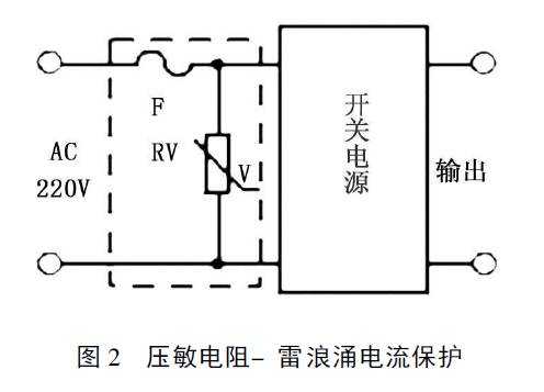
When the power transmission line is subjected to lightning strikes or induced lightning, the induced abrupt voltage in the transmission line will generate a surge current. In order to prevent lightning surge voltage and current surge, one or several varistors are often connected in parallel with the input of the power supply to release the lightning surge current. Figure 2 circuit uses varistor to prevent lightning surge current, varistor Rv is high impedance (approximate open circuit), when the power transmission line encounters lightning strike or inductive lightning, the varistor Rv instantaneously exceeds it The starting voltage, it will immediately change from high impedance to low impedance (approximate short circuit), which will release the lightning surge current, and the AC fuse F will be blown, which will prevent the transmission line from being damaged by lightning or inductive lightning.
LED semiconductor lighting network information For switching power supplies, safety and reliability have always been regarded as one of the important performance. The switching power supply can work safely and reliably under the condition that the electrical technical specifications meet the requirements of normal use of electronic equipment, and also meet the external or own circuit or load circuit failure. Therefore, various protection measures are required. Analysis of the characteristics of the protection circuit, and the lack of expectation to overcome, hope to design a safer and more reliable protection circuit.
1. Analysis of surge current circuit
The inrush current is caused by a sudden change in voltage. For example, when the electronic device is applied with voltage for the first time, the initial current is injected due to the charging of the large-capacity power supply capacitor. The surge current is turned on; and the sudden change of the lightning strike and the induced lightning enters the switching power supply along the power line. The transient current generated by the voltage is the lightning surge current. The surge current rises very quickly, the duration is very short, and the damage is very large. In order to prevent or reduce the damage of the inrush current, set the way to suppress the inrush current or transfer the inrush current to the ground to protect the switching power supply from the inrush current.
1.1 Start current limiting protection
The primary rectifying circuit of the switching power supply has a large-capacity filter capacitor, and the rectifier tube charges the large capacitors at the instant of starting, so that the instantaneous current of the rectifier exceeds the rated value. In order to reduce the starting current limit (surge current), switching power supplies are usually equipped with anti-shock circuits. As shown in the circuit of Figure 1, at the instant of power-on, the voltage of the 3 and 4 windings of the switching power supply transformer is 0V, VD5 is cut off, and the voltage between the G and K poles of the thyristor VD6 is 0V, and VD6 is cut off. Charging current path: AC220V→VD1- 4 positive → large capacitance C1 → ground → R2 → VD1 4 negative. Since R2 has a large current blocking effect (generally set to 3.3 Ω??), it can effectively limit the starting surge current.


After the switching power supply works normally, the induced voltage is generated on the 1 and 2 windings of the switching power supply transformer, and C2 is charged (the charging time constant is approximately equal to R3×C2), so that VD6 is turned on, the rectified current is no longer passed through R2, but is passed through VD6. A, K pole return to the negative pole of rectifier bridge VD1 - 4. In other words, in normal operation, VD6 shorts R2 to prevent R2 from generating power. R2 only works at the moment of power on.
The use of thyristor as the starting current limiting protection is safe and reliable, but the circuit is more complicated. From the perspective of circuit cost and simple circuit, the temperature-controlled resistor is used for starting current limiting protection, which is economical, simple, safer and more reliable, as shown in Fig. 3.
1.2 lightning surge current protection
When the power transmission line is subjected to lightning strikes or induced lightning, the induced abrupt voltage in the transmission line will generate a surge current. In order to prevent lightning surge voltage and current surge, one or several varistors are often connected in parallel with the input of the power supply to release the lightning surge current. Figure 2 circuit uses varistor to prevent lightning surge current, varistor Rv is high impedance (approximate open circuit), when the power transmission line encounters lightning strike or inductive lightning, the varistor Rv instantaneously exceeds it The starting voltage, it will immediately change from high impedance to low impedance (approximate short circuit), which will release the lightning surge current, and the AC fuse F will be blown, which will prevent the transmission line from being damaged by lightning or inductive lightning.
1.3 Actual circuit analysis and simulation test
Figure 3. The circuit is a typical part of the actual switching power supply circuit.
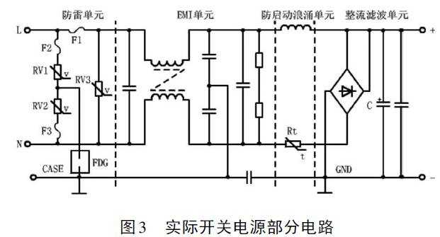
Lightning protection unit: When there is lightning strike, high voltage is generated through the power grid, and the circuit consists of Rv1, Rv2, Rv3, F1, F2, F3 and FDG. When the voltage applied across the varistor exceeds its operating voltage, its resistance decreases, so that the high-voltage energy is consumed by the varistor. If the current is too large, F1, F2, and F3 will burn out the circuit of the protection stage.
Anti-boot surge unit: When the power is turned on, it is necessary to charge C. Because the instantaneous current is large, its energy is completely consumed on the temperature control resistor Rt. Since the characteristic of Rt is exponentially decreasing with the temperature rise resistance (Rt is negative) Temperature coefficient component), Rt resistance decreases (low impedance) after the transient temperature rises, then the energy consumed is very small, and the latter circuit can work normally. The temperature-controlled resistor Rt changes from high impedance to low impedance, effectively preventing inrush current.
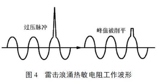
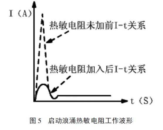
Simulation experiment: Using the lightning surge current generator to simulate the protection circuit before and after the experimental test waveform is shown in Figure 4 and the startup surge current test waveform is shown in Figure 5. Simulation experiments show that the common point of inrush current is that the action time is short (several to several tens of nanoseconds), and the inrush current is large (the lightning surge current can reach several tens to several thousand amperes, and the starting surge current exceeds the working current by several tens of More than double), the spike is cut off after adding the protection circuit.

2. Analysis of overcurrent protection circuit
It is well known that when the power output exceeds the rated load or the short circuit or the control circuit loses control and other unexpected conditions, the electronic device may not work properly or cause damage to the electronic device. The overcurrent protection circuit has a circuit breaking method and an oscillator frequency modulation method.
2.1 Open circuit overcurrent protection
The most economical and convenient way to protect against current overcurrent in the circuit is to use a fuse. Fuse blow protection is divided into AC insurance and DC insurance. When the load current is unexpected and its current exceeds the fuse's blown value (the fuse factor is generally between 1. 1 and 1.5), the fuse is blown to achieve overcurrent protection. However, at the moment of power-on, due to the charging of large capacitors, a large inrush current is generated. This surge current is generally several times the normal input current, which easily causes the fuse to blow, and a misjudgment occurs, which is its main defect.
2.2 Oscillator frequency modulation overcurrent protection
The so-called frequency modulation method is to generate a control signal by detecting the comparison amplifier circuit to change the oscillation frequency of the oscillator, so that the load voltage is reduced, thereby achieving the purpose of reducing the load current. Generally, the overcurrent protection setting value is 110% to 130% of the rated current, which can be automatically restored.
Under the coupling of the transformer, if there is an overload or short circuit at the output, the primary current will increase rapidly, and the voltage VRS on the detection resistor RS (manganese copper wire) will increase. In Figure 6 (A), the voltage VRS exceeds the B-E turn-on voltage of V2, and V2 is turned on. Since the V2 collector is connected to the control terminal of the oscillating circuit, the oscillation of the oscillating circuit is slowed or the oscillation is stopped. In Figure 6 (B) VRS output a control signal to the oscillating circuit after the voltage comparator, adjust the oscillating frequency, reduce the output voltage, reduce the load current, and achieve the purpose of protection. The overcurrent protection of Figure 6(B) and Figure 6(A) is more accurate, because the (B) circuit is designed with error comparison and error amplification circuits.
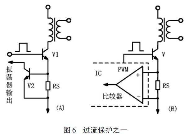
Figure 7 shows the constant current overcurrent protection circuit. In the circuit, R1 and R2 divide the VR, the voltage VR2= VR[ R2/ ( R1+ R2) ] on the resistor R2, the load current I0, the voltage VS= I0RS on the resistance RS, and the voltage VS and VR2 are compared. If VS>VR2, A outputs a control signal to change the frequency of the pulse signal, causing the output voltage to drop and the output current I0 to decrease.
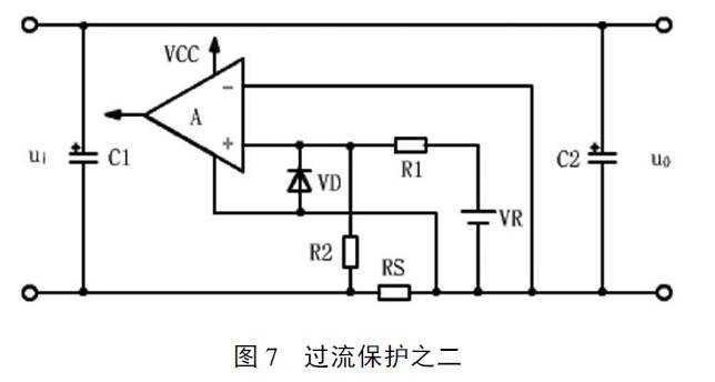
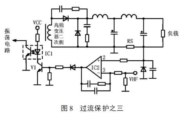
Figure 8 is a common optocoupler driven overcurrent protection circuit. Its working principle: When the output current is too large, the voltage across RS rises, the IC22 pin voltage is higher than the 3-pin reference voltage, IC2 outputs high voltage, and V1 turns on. The photoelectric coupler IC1 generates a photoelectric effect, which changes the oscillation frequency of the oscillation circuit, thereby controlling the width (or frequency) of the pulse signal of the switch tube to change, so that the output voltage is lowered, and the output overload current limit is achieved.
2.3 Insufficient
The sense resistor RS is always in the circuit. If the sense resistor RS value is small, the circuit protection response speed is not fast, and the accuracy is not too high. If the sense resistor RS value is too large, the power consumption will increase significantly, and the sense resistor RS There is reactive power loss to reduce the efficiency of the switching power supply. In order to reduce the reactive power loss of the detection resistor RS, a circuit such as a detection signal amplification is adopted to improve the reaction speed and accuracy of the protection circuit.

3. Analysis of overvoltage protection circuit

Switching power supply circuit overvoltage is divided into power supply external overvoltage and internal overvoltage, they will make the electronic equipment work abnormally or burn out the electronic equipment. The overvoltage of the power supply mainly has the wrong voltage of 380 V; the internal overvoltage mainly comes from the abnormal circuit of the switching power supply itself or the component damage (loss of voltage regulation control) makes the output voltage too high. The most common overvoltage protection circuits are the open circuit method and the switch-off method.
3.1 Open circuit overvoltage protection
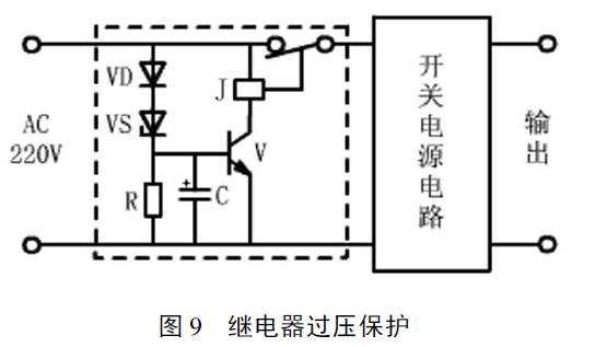
The external overvoltage mainly comes from the voltage of the power frequency grid is too high, such as the voltage of 380 V connected by mistake, as shown in Figure 9 is a circuit protected by the relay J shutdown circuit. When the AC power is normal, the current through the Zener VS is small, IRR < VbeQ, so the transistor V is turned off, and the relay J is in the normally closed (on) state. For some reason, when the AC power supply is higher than the normal state, the current through the Zener diode VS is very large, IRR> VbeQ, causing the transistor V (saturation) to conduct, the relay J acts, and the input circuit is cut off, thereby achieving the protection of the switching power supply circuit. And the load circuit. When the AC power returns to normal, the transistor V is turned off and the relay J is in the normally closed (on) state. The advantage is that the power supply can be automatically restored. The disadvantage is that the stability is poor and the size of the relay J is large.
3.2 Switch tube cut-off method overvoltage protection
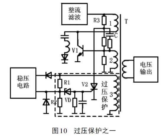
The switching power supply itself has abnormal circuit or component damage (loss of voltage regulation control) makes the output voltage too high. Figure 10 shows the overvoltage protection circuit driven by a thyristor. Under the normal voltage output condition, the negative voltage of the upper and lower ends of the third winding of T803 can not make VD breakdown through the voltage division of R1 and R2, and the thyristor V2 is also cut off, and the protection circuit does not operate. For some reason, the switching tube V1 loses the voltage regulation control, and the output voltage rises abnormally. The voltage of the third winding of the high-frequency transformer T will exceed the breakdown voltage value of VD after being divided by R1 and R2, causing the VD to break down and cause the thyristor. V2 triggers conduction. After the thyristor V2 is triggered, the upper end of the capacitor C is grounded, and the switch V1 is quickly turned off. After the third winding voltage of the high-frequency transformer T is rectified, the output of the voltage regulator circuit can be weakened by the oscillation control signal, and the switching tube V1 is further accelerated. After the protection circuit is activated, since the rectified and filtered DC voltage is supplied to the A pole of the thyristor V2 via R3, V2 will be turned on continuously until the fault is removed and the power is turned on again, and V2 is turned off.
As shown in Figure 11, an overvoltage protection circuit driven by a photocoupler is shown. Among them, the optocoupler IC1 plays two roles in the switching power supply. One is to implement a solid state relay; the other is to isolate the input and output.
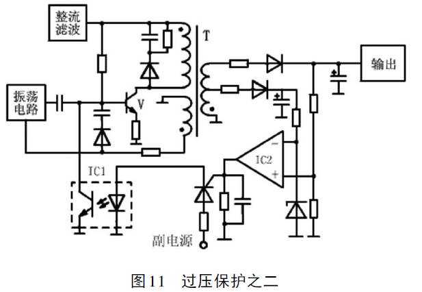
When the output voltage exceeds the normal value, the internal light-emitting diode of the photocoupler IC1 is illuminated by the error comparison amplifier IC2, so that the internal phototransistor of the IC1 photocoupler is saturated and turned on, so that the V-pulse current of the switch tube is photo-transistor Short circuit, so the switch tube V is quickly cut off. After the protection circuit is activated, the thyristor will be turned on continuously due to the A-pole power supply of the secondary power supply DC voltage thyristor, and the phototransistor is also saturated and turned on until it is turned on again.
3.3 Insufficient
Since the switch is turned off, there is no output voltage. However, when the input is connected to the wrong line and the voltage of 380 V is introduced, the voltage applied to the components such as the filter capacitor and the switch tube is still 380 V. If the voltage resistance of these components is insufficient, it is damaged.

4, the actual circuit analysis
Figure 12 shows an actual switching power supply circuit. The 220 V AC power is rectified and filtered to obtain a DC voltage of about 300 V, which is then applied to the V3 (high-power switch) collector via the 5 and 1 windings of T3. L22, L23 can continue the impact of pulse current on the V3 electrode, C23, C24 can absorb the V3 collector spike to prevent V3 breakdown damage. The 9 and 7 windings of T3 are positive feedback windings, and the feedback potential is coupled to the base of V3 via R26 and C19, so that V3 generates self-oscillation and the oscillation frequency is 30-60 kHz. VD39 provides a discharge loop for the positive feedback coupling capacitor C19, while limiting the b-e pole reverse voltage of V3 during the deadline to zero. 7 V to prevent b-e breakdown of V3.
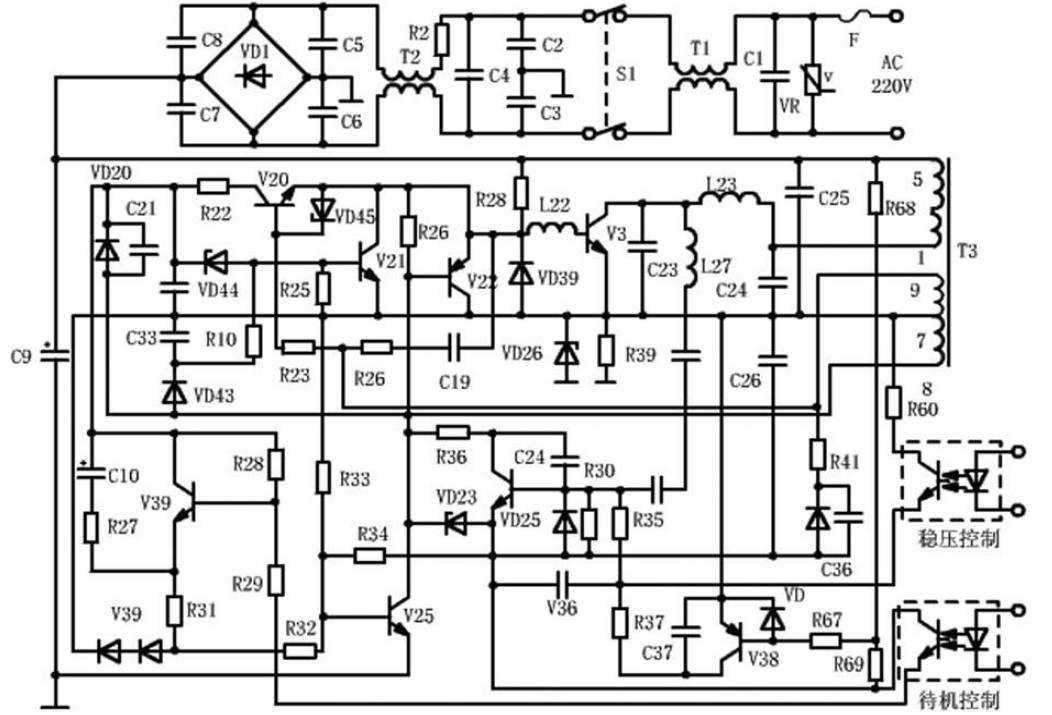
V20 is a constant current drive tube. The 8 and 7 winding potentials of T3 are filtered by VD20 and C21 capacitor to establish a DC voltage of about 8 V. This voltage is supplied to the V20 collector via R22. During the saturation of the switching transistor V3, the potential of the 9th terminal of T3 turns on V20 through R23, so V20 provides a constant current driving current for V3, and its size is determined by the resistance of R22. The constant current driving expands the AC input voltage range of the switching power supply to 90- 270 V.
V21 has two functions. The first is overvoltage protection. When the voltage across C21 rises from the normal value of 8 V to 10 V. VD44 breaks through and causes V21 to turn on. The V3 base excitation current is short-circuited by the ce pole of V21, which protects the switch V3 from the off state. The second function is to delay control of V3 conduction. During the V3 cut-off period, the positive potential of the 8 terminal of T3 and the negative potential of the 7 terminal charge C33 through VD43. When V3 is turned from the off state to the saturated state, the charging voltage of C33 will maintain V21 for a certain period of time. During this period, V21 shunts the excitation current of the V3 base, that is, delays the conduction of V3 for a period of time. At this time, the V3 collector voltage has dropped to a low point to reduce the power generated by V3 from the turn-off to the saturation state. loss.
V38 is the undervoltage protection control tube. First, the 7th terminal of T3 is positive potential, the 9th terminal is negative potential, and VD24 rectifies and establishes about 10 V DC voltage on C26. This - 10 V voltage is applied to V38 via R69 and R67. The base. In addition, a 300V voltage is applied to the V38 base via R68. When the input AC voltage is lower than 110 V, that is, the DC voltage obtained after rectification and filtering is reduced from 300 V to less than 150 V. At this time, the base potential of V38 is also lowered, and then V38 is turned on, and then V24 and V22 are turned on. The V3 base excitation current is bypassed by V22, which protects the switch V3 from the off state.
V25 is the overcurrent protection control tube, R39 is the overcurrent detection resistor of the switch tube V3, and the overcurrent voltage drop on R39 is applied to the base of V25 via R33, which causes V22 to turn on after V25 is turned on, so the switch tube V3 has passed The stream is in an off state.
All in one pc 23.8 inch, all in one pc i5 8gb ram, all in one desktop intel core i5, pc all in one 24 inch
Guangdong Elieken Electronic Technology Co.,Ltd. , https://www.elieken.com