Technological progress and market demand are the two driving forces for the development of the LED industry. LED packages have undergone a history of traditional and packaged flip-chip packages in a variety of package formats. With the changes in market demand, LED chip preparation technology and LED packaging technology, LED packaging will mainly develop in the direction of high power, multi-chip integration, high light efficiency, high reliability and miniaturization.

From the development history of China's LED packaging, there are several structures such as LED chips for traditional dressing, LED chips for Flip-Chip packaging, and LED chips for leadless flip-chip packages. Leadless flip-chip LED packages Technology is the mainstream technology for LED packaging in the future.
First, the development history and development trend of LED packaging
With the development of chip technology and the market demand for higher brightness, various forms of package products have been produced in large quantities, from early lead-type LED devices, chip printed circuit board (PCB) structures, polyphthalamide ( PPA), poly(ethylene terephthalate) (PCT) and thermoset epoxy resin (EMC) structure LED devices to today's aluminum nitride ceramic structures, high power integrated chip-on-chip packages (ChipOnBoard, COB ), each Different types of packages such as flip chip. The evolution of China's LED package form is shown in Figure 1.
In the future, LED packaging will focus on lighting applications, mainly in the direction of high power, miniaturization, multi-chip integration, high light efficiency and high reliability. In order to improve the lumen efficiency of white LED devices, solving technical problems such as heat dissipation, high light efficiency and high reliability of packaged devices under high current and high power operating conditions will become a new topic.
Second, the advantages and disadvantages of dressing and flip chip packaging
The LED package can be easily divided into a packaged chip package and a flip chip package. The flip chip package is further divided into a leaded flip chip package and a leadless flip chip package. The flip chip package is a packaging process that utilizes LED flip chip and various packaging materials to effectively combine into a product through a specific technical solution. The reason why flip chip is called "flip-chip" is relative to the process of mounting a wire bonding method. The LED chip of the package is facing up, and the electrical face of the LED flip chip is facing downward, which is equivalent to turning the former over, so it is called "flip chip", and the light of the flip chip is taken out from the sapphire substrate. It is not necessary to take it out from the current diffusion layer, and the opaque current diffusion layer can be thickened to increase the current density.
1, LED dressing chip package
The positive-package chip package uses silver glue or white glue to fix the chip on the substrate, and electrical connection is made through the leads. Silver or white glue contains epoxy resin, which has poor long-term environmental stability and high thermal resistance. The adhesive strength gradually deteriorates during long-term energization of LED, which leads to shortened LED life; and the lead wire is very thin and resistant. The current impact capability is poor, and can only withstand a force of about 10g. When subjected to thermal shock, the thermal mismatch of various packaging materials may cause the lead to break and cause LED failure. The single LED chip assembly structure is shown in Figure 2.
The advantages of LED packaged chip package are: 1 chip preparation process is mature; 2 packaging process is relatively mature.
The disadvantages of LED packaged chip package are: 1 electrode, solder joint, lead shading; 2 long heat conduction path: sapphire adhesive support metal substrate; 3 low thermal conductivity: sapphire thermal conductivity 20W / (m · K), bonding The thermal conductivity of the glue is 2W/(m·K); 4 heat accumulation affects the reliability of the chip and the phosphor.
2, leaded flip chip package
The leaded flip chip package is to fix the LED flip chip on the substrate through the thermal conductive adhesive, and then electrically connect by using the gold wire. The flip chip is a flip chip mounted on a silicon (Si) substrate by means of a gold ball, and an electrode is prepared on the Si substrate to form a flip chip. A leaded flip chip package structure is shown in Figure 3.
The advantages of leaded flip chip package are: 1 sapphire substrate upward, no electrode, solder joint, lead shading, light extraction efficiency; 2 heat transfer effect is good, easy to conduct.
The disadvantages of leaded flip chip package are: 1 long heat conduction path: metal solder joint → silicon substrate → thermal conductive adhesive → bracket heat sink; 2 with lead connection, limited current carrying capacity, reliability caused by lead soldering problem.
3, leadless flip chip package
The leadless flip chip package is a method in which a horizontal electrode chip in which an electrode contact surface is plated with an alloy such as tin (Sn) or gold (Au)-tin is directly soldered to a substrate plated with gold or silver by a eutectic/reflow soldering technique. The chip is fixed and electrically connected and thermally conductive. The leadless flip chip package structure is shown in Figure 4.
The advantages of leadless flip chip package are: 1 no electrode, solder joint, lead shading; 2 no lead hindrance, can realize flat coating phosphor and ultra-thin package; 3 electrical connection is surface contact, can withstand high current impact; 4 Short heat conduction path: gold solder joint → aluminum nitride ceramic/metal substrate; 5 metal interface has higher thermal conductivity and smaller thermal resistance; 6 completely free from the binding of lead and adhesive, showing excellent strength, heat and light Electrical performance.
Third, the future leadless flip chip package
With the development of epitaxy, chip preparation technology and IC chip-level micro-packaging technology in LED, flip chip-based leadless packaging technology will become a new LED packaging technology leading the market in the future.
At present, there are chip and packaging manufacturers in the development and industrialization of leadless packaging technology, mainly in the following two ways: one is that the chip manufacturer directly makes LED chip-level devices that have been coated with phosphors, and the LED chip-level devices can be The light source board (such as Figure 5) is directly soldered to the circuit substrate by a die-bonding reflow process, such as CREE XQ-E, Samsung LM131A, and Crystal 16×16 package-free chip products.
The other is that package manufacturers use eutectic/reflow-like methods to package horizontal electrode flip-chips from chip manufacturers into various leadless package products (Figure 6), such as Jingke Electronics (Guangzhou) Co., Ltd., Taiwan Long Power Electronics Co., Ltd. and Shenzhen Tiandian Optoelectronics Technology Co., Ltd., Jiangxi Jingrui Photoelectric Co., Ltd. and other ceramic substrates 3535, 2016, high-power COB and other power-type packaging products.
Conclusion
At present, the flip chip-based leadless packaging technology is mainly applied to high-power products and multi-chip integrated package COB products. In the application of small and medium power products, its cost competitiveness is not very strong. Although the LED leadless flip chip package is subverting the traditional LED package process, other package forms will still exist in order to meet the application structure requirements of the product structure.
At present, the technical route of the leadless flip chip packaging process has been clarified, and the related equipment and processes will be updated. Although the packaging process cost is high, and the current brightness has no obvious advantage compared with the conventional package, there are many other products because of the leadless flip chip package. The advantages will still be the development trend of semiconductor lighting LED packaging technology. All kinds of LED leadless flip chip packages have been applied in indoor and outdoor lighting, decorative lighting and backlighting. With the emergence and advancement of new technologies and the expansion of technology applications, especially in the promotion and mature application of small and medium power packages, The leadless flip chip package will further highlight the cost and technical advantages, become the mainstream of technology, and lead the industry.
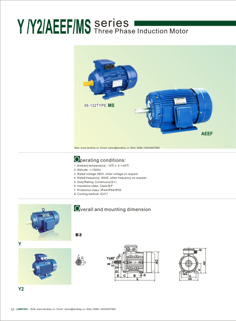
MS Three-Phase Aluminum Housing Electric Motor
MS Series 3-phase Aluminum Housing Induction Motor
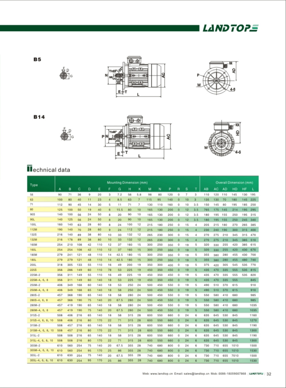
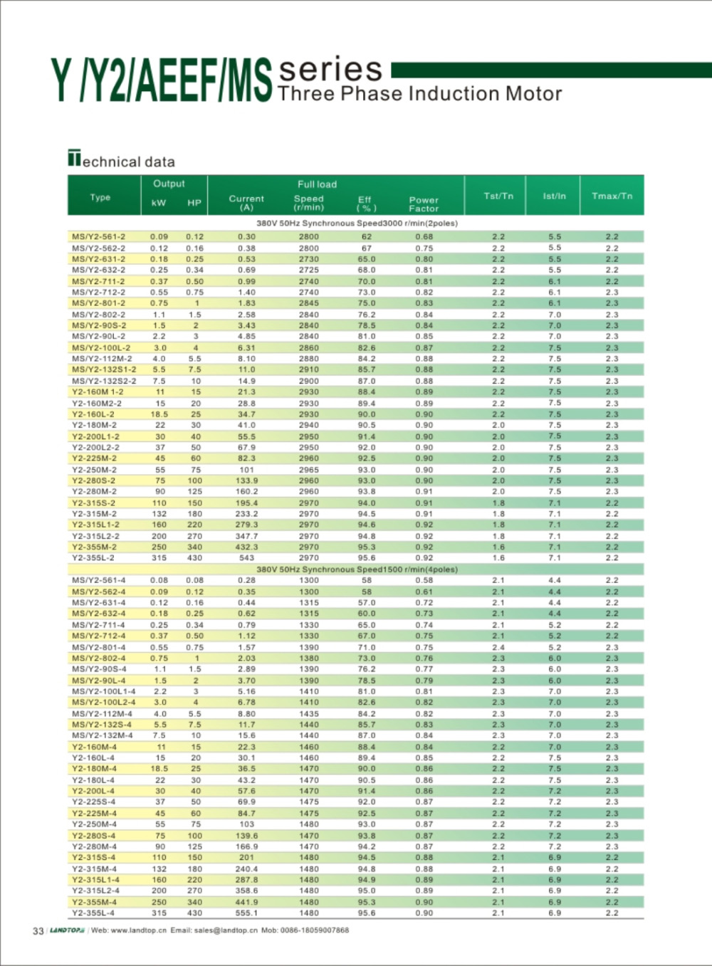
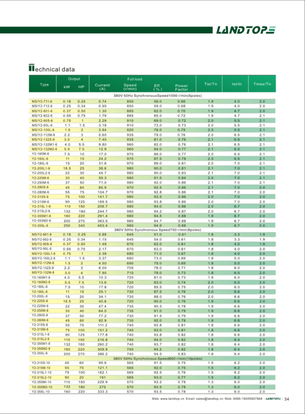
MS series motor is totally enclosed and fan cooled 3 phase squirrel cage induction motor. It is newly designed in conformity with the relevant rules of IEC&DIN42673 standards. Y connection for motor of 3kw and below. Delta connection for 4kw and above.
Application:
MS serise 3 phase motors are widely used as driving equipments of various machineries such as: machine tools, blowers, pumps, compressors, transporters, agricultural and food processing.
Operating Condition:
Ambient temperature: -15°c to 40 °c
Altitude: ≤1000m
Rated voltage: 380V, 400V, 415V, 220V, 230V, 240V, etc
Rated frequency: 50HZ, 60HZ, 50HZ/60HZ
Duty: Continuous(S1)
Insulation class: Class B, Class F
Protection class: IP44, IP54, IP55
Cooling method: IC0141
Note:
The voltage and frequency could be made according to your request. If there is any requirements or inquiries, welcome to contact us.


MS Three-Phase Electric Motor,10KW Electric Motor,3 Phase AC Motor,Three Phase Electric Motor
FUZHOU LANDTOP CO., LTD , https://www.landtopcos.com