This kind of system control method is not suitable for applications such as precise motion control (such as precise control of the rotational speed of the motor with varying load) because they require a short communication delay between the controller and the equipment, but it requires a highly synchronous system level control. Accurate control of the entire system (such as a speed change), such as a large printing plant or a long automated production line, is useful. If there is enough time for each device to issue an instruction, the only constraint on such clock-based control accuracy is system-wide clock synchronization accuracy.
Several industrial networking standards (not just Internet-based standards) are using the IEEE 1588 standard to provide this control capability. IEEE 1588 provides a highly accurate master clock and a validated clock synchronization mechanism that can be used to generate all local clocks and maintain very accurate system-level synchronization with the master clock.
Ethernet-based networks are favored for their low cost and ease of implementation of Ethernet. Ethernet switches are key components that help these advantages, and enterprise systems rely heavily on them for high-performance and easy-to-maintain infrastructures. This huge enterprise market for switches means that they are easy to implement and inexpensive, but most switches on the market today are not designed for low latency performance or deterministic routing times, and are therefore difficult to use in industrial environments.
The IEEE 1588 system synchronizes the master and slave clocks by detecting the communication delay between the master and the slave. Placing a switch between the master and slave clocks introduces additional delay because the switch must analyze the packets and then route them. The increased delay is not a good thing, but it can be corrected for delays, so it is not a major issue. The biggest problem is that as traffic increases, the time required to route packets will increase dramatically.
This is due to the time required to cache, analyze, and route packets to many destinations. This change greatly reduces the accuracy of the 1588 clock synchronization, which significantly deteriorates the real-time control performance of the entire system. The measurement of the delay between 1588 master and slave clocks also depends on the symmetry of the communication time in both directions because the measurement method used is to count a time stamped message from the slave clock to the master clock and then back from the master clock to the slave clock. The time used is divided by 2. In most switch and Ethernet network implementations, this symmetry is less likely to occur, further reducing clock synchronization accuracy.

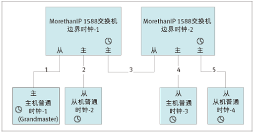
Figure 1: Typical Boundary Clock Application Diagram
However, the IEEE 1588 standard provides a solution to this problem: If the switch itself also has a clock (shown in Figure 1), it can measure the time required for packet routing and integrate it into the synchronization calculation. Because the system does not need this functionality, switches that contain such 'boundary' clocks are difficult to see, and are generally expensive, and are often customized for specific network implementations. With the rapid proliferation of IEEE 1588-based networks, manufacturers face daunting challenges in how to implement IEEE 1588 functionality efficiently and cost-effectively in product and network infrastructures.
Developing a custom ASIC solution is possible, but with the rise of ASIC development costs and rapid changes in industrial Ethernet standards, the development of such programs is slow, risky, and not cost-effective. Solutions can also be developed for each protocol using microprocessors and third-party ASICs or ASSPs for specific network protocols, but this means implementing a separate solution for each network standard, which is also costly and inefficient. These solutions may also face the problem of lack of flexibility and equipment quickly out of date.
At present, designers can only avoid the above restrictions by carefully implementing networks, minimizing the use of switches, or minimizing real-time network traffic. This network isolation measure can achieve acceptable performance levels for some applications, but they are difficult to implement or maintain.
Save development time
Implementing IEEE 1588-enabled switches with FPGAs is the ideal solution to this problem. Directors of Altera, National Semiconductor and MorethanIP have combined their expertise to provide an optimized eight-port switch design for industrial Ethernet designers. This design can reduce engineering development time by six to nine months. The savings in development time will enable device manufacturers to take the lead in time to market.

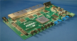
Figure 2: Eight-port switch development board with IEEE 1588 timing control
Figure 2 shows a development board with embedded IEEE 1588 capabilities developed by Altera's Stratix II FPGA based on the MorethanIP enterprise system. The reference design attached to this development board implements IEEE 1588-compliant switches in a simple and cost-effective way, and is easily modified to cater to other systems and rapidly changing market demands. These advantages are achieved through the flexibility of the FPGA and a 32-bit RISC processor integrated in the FPGA design.
The Ethernet MAC core and switching core intellectual property (IP) with 1588 timing control and programmable uplink functions was developed by MorethanIP GmbH. The MorethanIP Enterprise System also provides UDP and 1588 software stacks that can run on a 32-bit Altera Nios II RISC processor soft core. To provide the best physical interface, the eight-port switch design uses four dual-port PHY transceivers from National Semiconductor Enterprise Systems.
The reference design has less than 100ns clock synchronization capability and can be used in a variety of applications. This level of accuracy is critical to meeting the demanding communication delays and quality of service (QoS) requirements for industrial connectivity. Target applications include switches using different industry standards such as Ethernet/IP, ProfiNet, Ethernet Powerlink, and other Ethernet protocols.
Extend product life cycle
The FPGA's programmability is the key to the above design advantages. From a single hardware platform, designers can easily implement switches that support different industrial Ethernet protocols (such as EtherCAT, ProfiNet, etc.). The board can support different industrial Ethernet protocols within the same system or from the same Ethernet port.
This is achieved by implementing different media access controller (MAC) hardware modules and embedded processor software to support different Ethernet standards and IEEE 1588 functions. The ability to easily reuse previously designed capabilities and the availability of off-the-shelf IP means that FPGA-based designs can generate a configuration that supports new features in a very short time compared to designs using ASIC or ASSP devices.
The FPGA loads hardware configuration and embedded processor software from a serial flash. Even after the device is delivered to the site during production, it is easy to change the hardware and software functions of the FPGA by rewriting the contents of the flash memory.
The programmable hardware and software processing power within the FPGA means that designers can integrate the additional functionality they need through applications that are hardware or software. The ability to implement new functions by simply reprogramming the FPGA is a guarantee of the future of the product (such as support for IEEE 1588 v2.0), and new features can be presented to customers very quickly.
Because of the long lifecycle of FPGAs, device manufacturers do not have to worry about the risk of potential device termination. Since the design is based on IP, porting the design to next-generation FPGAs is also more convenient, making it possible for designers to benefit from the lower cost or greater performance of next-generation FPGA products. Coupled with the ease of on-site upgrades, FPGA implementation becomes the best way to easily support product development throughout the product cycle.
This reference design uses Altera's Stratix II FPGAs, which allow all Nios II processor code to be stored in on-chip memory, although lower-cost systems can be implemented using the Altera Enterprise System's Cyclone III family of FPGA devices.
Embedded Switch Matrix IP
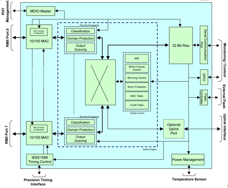
Figure 3 shows the embedded eight-port switch fabric of MorethanIP GmbH's enterprise system. It contains 8 10/100 Mbps MACs that conform to the Ethernet 802.3 specification and each MAC supports IEEE 1588, which means that it can use programmable timing. The local synchronous high-accuracy clock is time-stamped for each incoming 1588 data frame.

Figure 3: Block Diagram of MorethanIP's Eight-Port Switch Compliant with the IEEE 1588 Standard
To implement the boundary clock application, the switch design implements both IEEE 1588 V1 master and slave applications. The port that communicates with the host is automatically configured as a slave port. The embedded 1588 application generates a precise clock from the slave port and forwards the clock information to other ports that are automatically configured as master. Tight integration with programmable timers ensures that the clock is synchronized to the master clock within 100 ns.
Within the switch, up to two priority queues can be implemented per port to provide Quality of Service (QoS) guarantees for critical services. The switch can also programmatically identify and prioritize traffic using a 3-bit VLAN priority field, a 6-bit DiffServ Layer 3 code point (IPv4), or an 8-bit service class (IPv6).
The switch is designed to support IEEE 1588 Release 1 boundary and Release 2 transparent clock applications. The design can be further modified and enhanced to add custom logic, such as the addition of bridged application software on legacy system or PCI and other different system interfaces to facilitate the integration of switches into existing systems.

Figure 4: IEEE 1588 block diagram including software and hardware
In this design, the Nios II embedded processor supports the IP configuration and management of the switch, and can run the User Datagram Protocol (UDP) stack, the IEEE 1588 protocol stack, and precise timing synchronization, and supports dual 10/100 PHY transceiving. The PHY management and line diagnostics of the device (as shown in Figure 4). Embedded processors can also be used for high-level networking functions such as running spanning tree and rapid spanning tree algorithms and terminating TCP/IP links. Spanning Tree Protocol (STP) and Rapid Spanning Tree Protocol (RSTP) are link management protocols that support path redundancy to prevent unwanted loops in the network (so that industrial Ethernet networks work properly, only between two nodes. There can be a valid path).
PHY transceiver

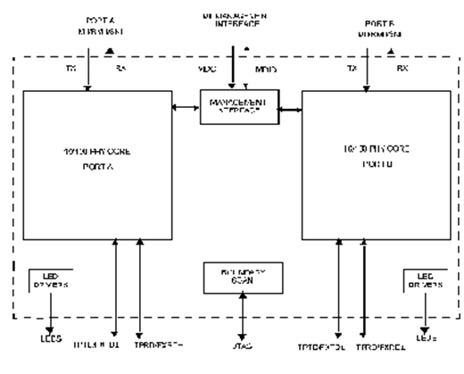
Figure 5: National Semiconductor's PHY Transceiver Block Diagram
Each transceiver has two completely independent 10/100Mbps ports for multi-port applications, as shown in Figure 5. The transceiver's port switching also allows the two ports to be configured to provide fully integrated range expansion, media conversion, fast hardware-based failover, and port monitoring.
The device incorporates multi-port support for a common industrial Ethernet topology. In particular, designers need redundant support for different applications and need to be able to handle failover under a variety of conditions. Switching from one network stack to another requires no less than a few hundred milliseconds, but some applications, such as security applications, require a failover that is extremely fast, preferably at the PHY layer. The transceiver in this reference design switches from one port to another in ns, even though the host still manages the control path. The architectural improvements in the transceiver signal path far exceed the minimum PHY layer specification requirements, and can completely solve design issues such as jitter and latency. Each Ethernet PHY layer is driven by a reference clock. In order to minimize jitter, the PHY layer specification requires an extremely accurate clock with accuracy within 50 PPM of the transceiver's 25 MHz reference clock. In addition, in order to meet the specification requirements, the starting jitter must be very small. To solve this problem, a mechanism that tolerates more jitter is integrated within the architecture. The device architecture also optimizes latency performance for real-time Ethernet operations to ensure that switch latency is minimized.
In many real-time system implementations, Ethernet packet data transmission delay is an important parameter for normal system operation, and fixed or variable delay in the Ethernet PHY will become an important component of system delay calculation. section.
The PHY transceiver is designed to limit the variation of the received data delay, which provides a very deterministic system delay. Because the receive data is aligned with the receive clock, the non-deterministic factors that are typically encountered when the device receives data are circumvented. Therefore, the device can provide very deterministic receive data delay in MII and RMII modes. In addition, the transceiver can reduce the non-deterministic possibilities common in sending RMII delays.
Another important design feature is the built-in cable diagnostics feature that adds a forward-looking diagnostic capability to the transceiver's traditional time domain reflectometry (TDR) approach. The newly created fault isolation feature can use the transceiver's powerful signal processing capabilities to track link quality while data is being transferred. This robust TDR implementation is to send pulses out of the receive or transmit wire pairs and observe the results on both wire pairs. By observing the type and intensity of the reflected signal on each pair of lines, and calculating by software, the short-circuit and open-circuit conditions of the cable and the distance of the fault point can be determined, and it can be determined which pair has the problem and the pair offset. Proactively monitoring and correcting changes or deteriorating link quality can reduce system downtime and save expensive maintenance costs. This function can also detect failures during installation and save a lot of debugging man-hours.
This article summary
Industrial Ethernet technology has been advancing and becoming more and more popular, and designers are facing increasingly strong demand for cost-effective industrial switches. Since ASIC and ASSP-based switches are fixed in their architecture, there is virtually no room for customization of new system features. In order to increase the design of features, it is generally necessary to overhaul them. This will lead to additional design time and cost. However, FPGA designs that support IEEE 1588 switches as described above can save engineering time by 6 to 9 months, and provide designers with the flexibility they need to help them implement the Precision Timing Protocol (PTP) and support multiple industrial Ethernet standards. , additional standard interfaces or other possible custom features.
Pin Header Connector,0.80Mm Header Connector,3.96Mm Pin Header Connector,Smt Vertical Type Connector
Shenzhen CGE Electronics Co.,Ltd , https://www.cgeconnector.com