Abstract: In digital communication systems, symbol synchronization plays a key role in achieving accurate signal decision symbols and reducing system bit error rate. This article describes the implementation of 16QAM receiver symbol synchronization algorithm in the ADS simulation environment. The timing error extraction algorithm used eliminates the clock jitter problem caused by the traditional algorithm in the 16QAM system and achieves the synchronization of the received signal and the transmitted signal. The algorithm is simulated in ADS environment. The simulation results show that the algorithm achieves the function of symbol synchronization and has strong resistance to interference.
0 PrefaceIn a digital receiver, in order to accurately determine the transmitted symbols at the moment of sampling decision, it is necessary to provide a timing pulse sequence that determines the timing of the sampling decision. The repetition frequency of this timing pulse sequence must be consistent with the transmitted digital pulse sequence (ie, the receiving and sending parties must be synchronized and have the same main frequency), and at the same time, the received symbols are sampled and decided at the best decision moment. Such a timing pulse sequence is called symbol synchronization.
16QAM (Quadrature Amplitude ModulaTIon) receiver to complete the demodulation of the 16QAM signal must first complete the symbol synchronization, and then complete the demodulation of the signal through the subsequent equalization, carrier recovery and other modules. Therefore, the implementation of the symbol synchronization algorithm is a crucial part.
1 Symbol Timing Synchronization Principle and Its Design in ADSIn the digital demodulator, the baseband signal obtained by down-conversion passes through a matched filter, and is sampled and quantized at a fixed sampling frequency with a clock cycle of Ts, and then enters a symbol synchronization loop.
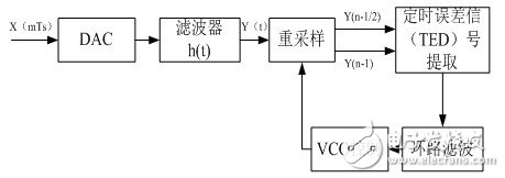
Figure 1 Structure of symbol synchronization module
In the paper, the specific timing synchronization module is shown in Fig. 1. It consists of an interpolation filter (equivalent to DAC, filter, and resampling), timing error extraction (TED), loop filter, and VCO control. Make up. It can be seen from the figure that after the signal is interpolated, there are two sampling points in each symbol, and then the clock error is extracted. The error signal obtained is sent to the VCO through the loop filter, and finally the interpolation is controlled to complete the synchronization. That is, the sampling clock is used to adjust the sampling clock to achieve synchronization.
The following describes the principle of each module.
1.1 Principle of interpolation filter
The interpolation filter actually implements a data rate conversion assuming its model is shown in Figure 2.

Figure 2 Rate conversion
Suppose the receiver has a fixed sampling clock ![]() The symbol period is T. The interpolator receives the signal as
The symbol period is T. The interpolator receives the signal as ![]() , After passing DAC and filter
, After passing DAC and filter ![]() , get a continuous time output:
, get a continuous time output:
 (1-1)
(1-1)
Now, for y (t), at every moment ![]() It is again sampled, where k is a positive integer. T is the interpolator cycle, which is synchronized with the symbol period.
It is again sampled, where k is a positive integer. T is the interpolator cycle, which is synchronized with the symbol period.
 (1-2)
(1-2)
For the above equation (5-2), m is the input sequence pointer and the filter pointer is defined as:
![]() (1-3)
(1-3)
Similarly, define the basic pointer as:
![]() (1-4)
(1-4)
The score interval is:
![]() (1-5)
(1-5)
The interpolation formula can be rewritten as:

(1-6)
Equation (1-6) is the basic equation of the digital interpolation filter.
Introducing parameters ![]() ,
, ![]() It is of practical significance. They represent
It is of practical significance. They represent ![]() ,
, ![]() The adjustment relationship between. among them,
The adjustment relationship between. among them, ![]() Determined to calculate the k-th interpolated value
Determined to calculate the k-th interpolated value ![]() N=N2-N1+1 signal samples,
N=N2-N1+1 signal samples, ![]() Indicate the interpolation evaluation point and decide to use it to calculate the interpolated value
Indicate the interpolation evaluation point and decide to use it to calculate the interpolated value ![]() The N interpolation filter impulse response samples. In general,
The N interpolation filter impulse response samples. In general, ![]() It is an irrational number and changes for each interpolation until the timing is stable.
It is an irrational number and changes for each interpolation until the timing is stable. ![]() Will be stable at a certain value.
Will be stable at a certain value.
1.2 Timing Error (TED) Signal Extraction
The Gardner symbol synchronization algorithm is an asynchronous clock recovery method that generates a symbol clock locally and uses the interpolation method to obtain the symbol value at the sampling time, and does not need to satisfy the requirement that the sampling clock and the symbol clock are integer multiples. In the Gardner symbol synchronization algorithm, the input baseband signal is interpolated to obtain sample data with a 2× symbol rate. The sampled data is controlled by the feedback branch to control the output frequency of the numerically controlled oscillator to adjust the symbol clock, and sampling is performed to obtain the best sampling point. Locking and tracking of the clock.
The Gardner algorithm does not require decision feedback. Each data requires two sampling points, one of which is the strobe point, which is the symbol's best observation point, and the other is the midstrobe point, which is the sampling point between the two best observation points. One is near the symbol decision point and the other is near the middle of the two symbol decision points, and is independent of the carrier phase deviation. Therefore, the timing adjustment can be completed before the carrier recovery, and the timing recovery ring and the carrier recovery ring are independent from each other, which gives the demodulator The design and commissioning bring convenience.
Assume that the received signal is: ![]() ,
, ![]() For transmitting complex data,
For transmitting complex data, ![]() Baseband filter waveform, right
Baseband filter waveform, right ![]() The sampling value may produce timing error, and the timing error extracted by the Gardner algorithm is:
The sampling value may produce timing error, and the timing error extracted by the Gardner algorithm is:

(2-1)
Where index r represents the number of symbols, the decision values ​​of the rth symbol in the in-phase I and quadrature Q directions are respectively expressed as ![]() with
with ![]() . Similarly, sample values ​​at the center positions of r and (r-1) decision points are represented as
. Similarly, sample values ​​at the center positions of r and (r-1) decision points are represented as ![]() with
with ![]() . The entire error is the sum of the timing errors in both directions I and Q, and this error is independent of the carrier phase.
. The entire error is the sum of the timing errors in both directions I and Q, and this error is independent of the carrier phase.
In the formula ![]() ,
, ![]() In-phase and quadrature components, T is the symbol period. The Gardner algorithm is suitable for tracking and capturing modes.
In-phase and quadrature components, T is the symbol period. The Gardner algorithm is suitable for tracking and capturing modes.
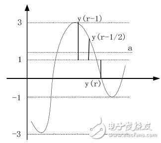
Figure 3 16QAM demodulated waveform
In the 16QAM modulation signal, if the sign changes from -1 to 1, 1 becomes -1, -3 becomes 3, 3 becomes -3, etc. When there is no timing error, the average value of the intermediate point should be zero. When there is timing error, a non-zero value will be generated, and its size is proportional to the size of the error. In other cases, the average value of the middle point is not zero when there is no timing error. For example, the sign changes from 3 to -1. When there is no timing error, the average value of the middle point is 1, as shown in FIG. 3 .
If the Gardner algorithm is used directly in the 16QAM demodulation system, the results of the timing error detection are somewhat correct and some are wrong. For a large amount of data, the average of these errors is zero because, in the absence of timing error, the midpoint may be 0, -1, 1, -2, 2, with an average of zero. Therefore, these errors can cause jitter in the timing clock, which can be reduced by the filter.
To eliminate these jitters. We have further improved the Gardner algorithm. The improved algorithm is:

(2-2)
among them ![]()
When the timing advances, the error is negative, the timing lags, and the error is positive. The Gardner algorithm has two characteristics: First, each symbol requires only two sampling points, and the error signal is output at the symbol rate; second, the estimation algorithm is independent of the carrier phase and is not affected by the carrier phase offset, ie, Prior to carrier phase synchronization, timing error estimation is performed.
1.3 VCO Voltage Controlled Oscillator
The interpolation filter of the timing recovery loop is controlled by the VCO, which accepts the timing error signal and provides the interpolating filter with the parameters required for the interpolation operation. ![]() with
with ![]() , VCO clock frequency is 1/
, VCO clock frequency is 1/ ![]() .
.
VCO output frequency f(m):
![]() ,
,
![]() Set the basic frequency for the VCO,
Set the basic frequency for the VCO, ![]() For the VCO control signal, the timing error signal is filtered by the loop filter and the output frequency of the VCO is
For the VCO control signal, the timing error signal is filtered by the loop filter and the output frequency of the VCO is ![]() The changes will change when
The changes will change when ![]() When stable, the output frequency will remain stable. S is the sensitivity of the VCO to the error signal. Each time a zero-crossing occurs at the VCO output, a timing-adjusted sampling pulse is generated
When stable, the output frequency will remain stable. S is the sensitivity of the VCO to the error signal. Each time a zero-crossing occurs at the VCO output, a timing-adjusted sampling pulse is generated ![]() So that you can decide
So that you can decide ![]() , which is to determine which sampled signal values ​​participate in the interpolation operation.
, which is to determine which sampled signal values ​​participate in the interpolation operation.
1.4 Loop Filter
The second-order digital filter is used to filter the timing error signal as shown in FIG. 4 to reduce the jitter of the timing error signal. Loop Filter Coefficient and Timing Error S-curve Coefficient and Numerical Control Oscillator Control Sensitivity Together Determine Loop Relative Equivalent Noise Bandwidth ![]() .
.
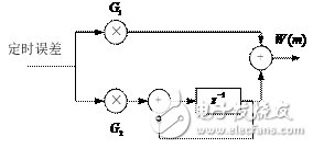
Figure 4 Second-order digital filtering
Selected loop relative noise bandwidth ![]() And damping coefficient, you can find the second-order digital filter parameters
And damping coefficient, you can find the second-order digital filter parameters ![]() ,
, ![]() .
.
ADS, short for HP Advanced Design System. It is a new set of circuit-aided design software from Agilent Technologies. Agilent Technologies integrated the existing products: HP MDS (Microwave Design System) and HP EEsof IV (Electronic Engineering Software) organically, and added many new features to form a powerful ADS software. ADS can be applied to the entire modern communication system and its subsystems, and can quickly and easily and effectively design and simulate the communication system.
ADS software is divided into Digital Signal Processing Network and Analog/RF Network two simulation design modules. The simulation of the receiver is done in the Digital Signal Processing Network, which loads a number of common communication devices that are available for recall.
In the ADS, a simulation model is established. This article simulates a digital demodulation system based on 16QAM modulation, 1.8GHHz IF, and 720Mbps code rate IF sampling (see Figure 5), and studies the key technologies for symbol synchronization in high-speed all-digital demodulation.

Figure 5 Communication System Bit Error Rate Simulation Project
Simulation design: 1. In the system, the symbol length is 5.6nsec. A delay of 2nsc was added to the LPT_RaiseCosineTImed filter at the transmitter to simulate symbol jitter.
2. Change the preset basic frequency of the VCO ![]() To simulate the receiver clock deviation, the VCO sensitivity S is 1MHz/V.
To simulate the receiver clock deviation, the VCO sensitivity S is 1MHz/V.
Simulation results:
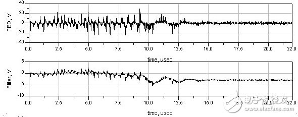
Figure 6 Error signal and loop filtered signal in the clock recovery loop
Figure 6 shows the error signal and loop-filtered signal measured from the symbol synchronization module. It can be seen from the figure that the VCO can adjust the sampling frequency in real time according to the feedback error signal after filtering (as shown in Figure 6) until the VCO output clock frequency ![]() Equal to 2 times the symbol rate, it reaches the equilibrium state, at this time the timing error is zero (as in Figure 6).
Equal to 2 times the symbol rate, it reaches the equilibrium state, at this time the timing error is zero (as in Figure 6).
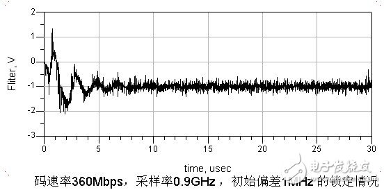
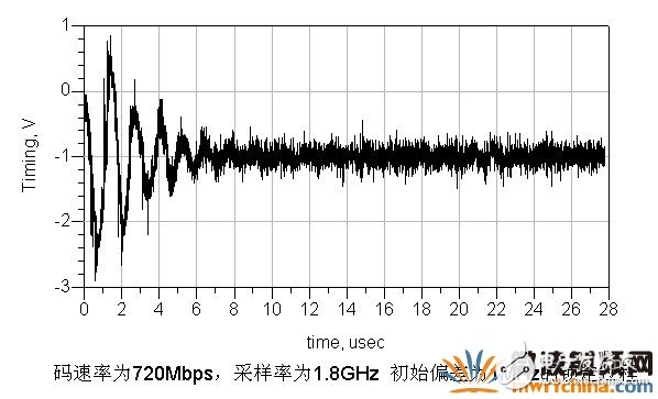
Figure 7 Locking process with different symbol rates
Figure 7 shows the 1.8GHz sampling rate, the symbol rate of 720Mbps, the initial deviation of 1MHz, and the symbol synchronization at the signal-to-noise ratio of 20dB; and the 0.9GHz sampling rate, the code rate of 360MHz, the initial deviation of 1MHz, and the SNR of 20dB. Synchronization of the time code to lock the situation. Simulations show that this symbol synchronization method can correctly generate symbol clocks to meet high code rate requirements and adapt to different code rates. The symbol clock can be generated correctly to meet the high code rate requirements and adapt to different code rates.
test environmentWhen the test item has no symbol synchronization module Bit error rate (BER) When there is a symbol synchronization module Bit error rate (BER)
The ideal system 4.554E-64.554E-6
Jitter 8.730E-59.039E-6
Receive clock deviation Bias=0.5MHz 0.0174.554E-6
Bias=1MHz0.0364.554E-6
Bias=1.5MHz0.0414.554E-6
Bias=2MHz0.0540.065
Jitter and deviation 0.0481.937E-5
Table 1 Error rate of symbol jitter and clock deviation in the simulation system
According to the above table, in the system shown in FIG. 5 , the symbol synchronization module has a strong ability to correct the jitter of the signal and the frequency deviation of the receiving end clock. When the jitter is half the symbol length, the module reduces the bit error rate from 1.730E-5 to 9.039E-6. The clock frequency deviation correction capability is particularly prominent, and can be locked within a range of 3 MHz (748.5 MHz~751.5 MHz). When simultaneously adding symbol jitter and clock skew, the system also exhibits strong error correction capabilities.
3 ConclusionThis paper briefly introduces the design of a 16QAM receiver's symbol synchronization module in the ADS simulator to eliminate the problem of recovery clock skew and symbol jitter caused by the asynchronous I and Q signals. And for the 16QAM modulation, an improved error extraction algorithm is proposed. Simulation shows that it can meet receiver requirements at different rates.
Two - way trigger diode, also known as two - end ac device (DIAC), and two - way thyristor at the same time.Because of its simple structure and low price, it is often used to trigger the bidirectional thyristor, and can also constitute overvoltage protection circuits.Construction, symbol and equivalent circuit of a bidirectional trigger diode.
Also commonly used in the overvoltage protection, timing, shift equal circuit, Figure 2 is the overvoltage protection circuit composed of bidirectional trigger diode and bidirectional thyristor.When the transient voltage exceeds the DIAC and Ubo, the DIAC quickly conducts and triggers the bidirectional thyristor to also conduct, so that the following load is protected from overvoltage damage.
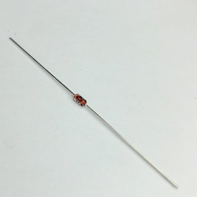
DO-35,DIACS,DO-35 Diode,DO-35 package,Small Signal Diode
Changzhou Changyuan Electronic Co., Ltd. , https://www.cydiode.com