A CMI coding design method based on FPGA and using Verilog HDL is implemented. The coding characteristics of the CMI pattern are studied, and the scheme of using the Altera Cyclone II series EP2C5Q FPGA to complete the CMI coding function is proposed. In the system programming, the m sequence is generated first, and then the program performs the CMI pattern transformation on the m sequence. In the CMI pattern conversion process, a special register is used to store the state of 1 code. At the same time, the m-sequence double frequency is used to provide clock excitation for the CMI encoding process, and finally the CMI code is output. The experimental results show that using FPGA to complete the design of CMI coding, the coding results are completely correct and can meet the expected requirements. Using this method to implement the CMI coding function has the characteristics of high efficiency, strong extensibility, and convenient upgrade, etc. It is convenient for embedding in large-scale design and has a wide range of application prospects.
The CMI code is generally used as a line pattern in a PCM4 subgroup digital trunk interface and an optical fiber transmission system. This type of code does not have a DC component, has more level jumps, and contains a wealth of timing information, so it is easy to extract the bit timing signal. This pattern has good error correction capability and is a very important pattern.
The CMI code is widely used as an interface code in high-end pulse code modulation terminal equipment, and is also recommended as a line transmission code in an optical fiber digital transmission system with a rate of less than 8 448 kb/s.
This article mainly introduces the specific implementation method of CMI code encoding. The system design adopts EP2C5Q FPGA of Cyclone II series of Altera Corporation as the core unit of the system to complete the CMI coding function. The program design platform is 0uartusII7.2 software and Verilog HDL is used as the program design. Language.
1 CMI coding rules and FPGA configuration circuitThe full name of the CMI code is the code inversion code. The coding rule of the CMI code is as follows: when 0 code is input, the code outputs 01; when code 1 is input, the code output is alternately 00 and 11 as shown in Table 1.
The rate of outputting CMI symbols according to this rule should be 2 times the symbol rate of the input baseband signal. For the input codeword of 1, the output is not only related to the current codeword, but also related to the output of the previous 1 code, and 1 code corresponds to The result of the coding is that the 00 or 11 pattern appears alternately. From the above rules, we can see that in the case of synchronization, the output only corresponds to 3 valid patterns. That is 01, 00, 11 code, and 10 code is invalid, so you can use this feature to detect errors.
The design uses Altera Corporation's EP2C5Q model FPGA, EP2C5Q is a CycloneII series of devices, CycloneII devices manufactured using 90nm process, in terms of logic capacity, PLL, multipliers and I/O numbers are better than Cyclone Great improvement. EP2C5Q model FPGA has abundant logic resources, a total of 4608 logic elements (LE), 26 M4K RAM blocks, 2 PLL phase-locked loops, and 13 18x18 multiplier modules.
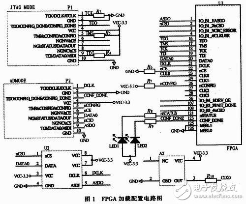
The problem that needs to be paid attention to in the FPGA hardware circuit design is the connection relation of JTAG download circuit, configuration chip EEPROM circuit and FPGA. Every time the FPGA is powered up, it needs to be configured, read data from the EEPROM, and start running. According to the role of FPGA in the configuration circuit, the configuration data can be loaded into the target device in three ways: FPGA active (AcTIve) mode; FPGA passive (passive) mode; JTAG mode. In FPGA active mode, the target FPGA actively outputs the control and synchronization signals (including the configuration clock) to Altera's dedicated serial configuration chips (such as EPCS1, EPCS4, etc.). After the configuration chip receives the commands, it sends the configuration data to FPGA, complete the configuration process. It should be noted that the active methods supported by Altera FPGAs can only be used with the active serial configuration chip (EPCS series) provided by Altera. This configuration mode is only supported in StraTIxII and Cyclone series devices (Cyclone and Cyclone II). In passive mode, other devices in the system initiate and control the configuration process. JTAG configuration mode JTAG is the standard interface for IEEE 1149.1 boundary scan testing. Most Altera FPGAs support configuration by the JTFAG port and support the JAM STAPL standard. Configurations from the JTAG interface can be downloaded using the Altera download cable through the Quartus II tool.
Figure 1 shows the FPGA configuration circuit diagram, including the FPGA (AcTIve) mode and JTAG mode loading circuit, and the connection relationship between the dedicated serial configuration chip EPCS1 and the FPGA.

In the process of system programming, the m sequence is used as the baseband input code, and then the program performs the CMI pattern transformation on the m sequence and finally outputs the CMI pattern. By analyzing the CMI encoding rules, 1-bit input symbols correspond to 2-bit output codes, so the CNI symbol output rate is twice that of the input m-sequence symbol rate. In program design, it is necessary to keep the m-sequence process clock as 2 times the clock of the CMI-encoded process. This is the prerequisite for completing the CMI-encoding task.
The m-sequence is the abbreviation of the longest linear feedback shifter sequence. The m-sequence has the characteristics of balance, run-length, linear superposition, auto-correlation and pseudo-noise. It is widely used. The m-sequence generated by the m-sequence generator is used as the CMI-encoded data source, and the 4-stage shifter is used to construct the m-sequence generator with the period P=24-1=15. The structure of the m-sequence generator is shown in Figure 2, where A0, A1, A2, and A3 represent one register, respectively.
When programming a m-sequence for CMI coding, the problem to be noted is that the output corresponding to 1 code is related to the state of the previous 1 code, so the state of 1 code is recorded so that 1 code corresponding to 00 is realized. Alternate output with 11 patterns.
The CMI coding system design software environment uses the Quartus II software platform. The Quartus II software is an integrated development tool that integrates all the tools and third-party software interfaces involved in Altera's FPGA/CPLD development process. By using this comprehensive development tool, designers can create, organize, and manage their own designs, including design input, synthesis, place and route, timing analysis, simulation, programming, and configuration. QuartusII supports multi-clock timing analysis, embedded SignalTapII logic analyzer, power estimator and other advanced tools, easy pin assignment and timing constraints, with a strong HDL synthesis capabilities.
SignalTapII Logic Analyzer is a very important test tool. It reads the hardware signal of FPGA and can capture and display the real-time signal behavior inside the FPGA, so that designers can intuitively judge whether the logic is accurate. SignalTapII functions like a logic analyzer, but compared with traditional logic analyzers, it has the following advantages: The use of SignalTapII logic analyzer does not consume additional I/O pins, if you use a traditional logic analyzer to observe the signal waveform, then The signal to be observed must be routed to the idle pin; the SignalTap II logic analyzer does not occupy space on the PCB. If a conventional logic analyzer is used, the test pin must be led from the FPGA device to the PCB. This increases the PCB trace difficulty. The SignalTapII logic analyzer also does not compromise signal integrity; the SignalTapII logic analyzer is integrated in the Quartus II software at no additional cost, while traditional logic analyzers are expensive.
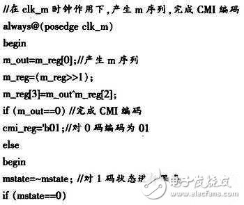
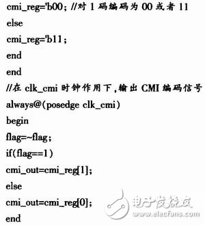
The program is designed using Verilog HDL language. Here is a partial source code for CMI coding:


There are two main processes in the program. The main function of the former process is to generate the m-sequence under the clk_m clock, complete the CMI encoding function, generate the m-sequence from the m_out output, and use the cmi_reg to store the CMI encoding value; the latter process is mainly The function is to output the CMI coded signal under the action of clk_cmi (which is twice the clock speed of clk_m).

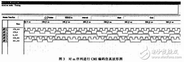
The Quartus II7.2 software platform was used to compile and simulate the CMI encoding program. The simulation results were obtained through simulation. Figure 3 shows the CMI code encoding simulation waveform.

From the simulation results, we can see that, under the trigger of the clock clk_m, the system outputs the m sequence from the m_out register and outputs a 15-bit m-sequence value, which in turn is 000111101011001; the system completes the CMI coding function under the trigger of the clock clk_cmi, and the CMI code The output value is then output by the cmi_out register. From the simulation waveform diagram, it can be seen that the output rate of the CMI-encoded symbol is 2 times the symbol rate of the m-sequence. The corresponding output values ​​are sequentially 010101110011000111010011010100, and the corresponding CMI coded signal has a certain time delay compared with the m sequence, but the encoding result is completely correct.
4 ConclusionThis article introduces the implementation method of CMI coding system using Altera's FPGA and Verilog HDL language. Altera's Cyclone II series EP2C5Q model FPGA has a rich logic unit. Through the Quartus II software synthesis simulation, you can see the program. The design only occupies 11 LEs, and less than 1% of LE resources occupy the FPGA. From the above simulation results, we can see that the coding result is completely correct and the design method described in this paper is reasonable.
The innovation of this system is that FPGA is used in the development of CMI coding logic, which makes the system design simple, the configuration more flexible, and easy to expand. It is free from the limitation based on the design of dedicated chips. The system uses FPGA as the core unit of CMI coding and applies Verilog. The HDL describes the CMI encoding logic and uses the SignalTapII tool to analyze the system logic. It has the characteristics of short development cycle, low cost, high efficiency, and convenient upgrade. The system also studied the m-sequence generator with a 4-stage shifter cycle of 15. The design method, which provides the source of information for the testing of the CMI encoder. The existing problem is that the system fails to reasonably select the FPGA model at the time of design, resulting in the use of FPGA resources is not reasonable. Therefore, in the FPGA-based system design process, in order to avoid waste of resources, it must be simulated through the simulation approach before design. Estimate the amount of resources needed for the design, and then select the corresponding FPGA model; but at the same time, we must pay attention to the capacity of the FPGA to leave a certain margin, because in the large-scale design, you can also design the CMI coding circuit and Other functional blocks are integrated in an FPGA, which is especially important when CMI coding is part of the system design.
ECG Trunk Cable,ECG Wire,ECG Patient Cable,ECG Lead Wire
Dong guan Sum Wai Electronic Co,. Ltd. , https://www.sw-cables.com