Summary
As the demand for data services accelerates, 4G technology will replace 3G as the mainstream wireless communication technology in the next few years, and TD-LTE with China's independent intellectual property rights will become an important part. This paper will introduce the commonly used transmitter architecture. And analyze the system indicators of TD-LTE transmitters, and combine TI's chip solutions to fully introduce the system solutions that support TD-LTE.
Term: DPD (Digital Pre Distortion)
Overview
TD-LTE with China's independent intellectual property rights has high spectrum utilization (downstream: 5bit/S/Hz; uplink: 2.5bit/S/Hz); high rate (downstream: 100Mbps; uplink: 50Mbps); low latency ( 100ms control plane, 10ms user plane), and flexible spectrum usage (variable bandwidth, 1.4MHz; 3MHz; 5MHz, 10MHz, 15MHz, 20MHz) are increasingly favored by various operators, by February 2011, by China Mobile led a joint 7 operators to launch the TD-LTE Global Development Initiative (GTI), which has grown to 48 operator members and 27 vendor partners; currently 38 operators plan to deploy or conduct trials.
This paper will analyze the challenges of transmitter systems (including transmission and feedback) of different architectures of TD-LTE, and finally decompose the system indicators according to the air interface indicators of TD-LTE, and provide ideas and basis for TD-LTE transmitter design. At the same time, combined with TI's scheme, the index requirements of key components of the transmitter link are analyzed.
1. Overview of TD-LTE transmitter architecture
In order to understand the system indicators of the base station transmitter system in more depth, this section will first introduce several architectures and their respective advantages and disadvantages commonly used in base station systems, so as to select different transmitter architectures according to different requirements.
In general, for TD-LTE, the biggest challenge now is bandwidth. China currently has 190MHz (2500-2690) continuous bandwidth allocated to TD-LTE, and there are many multi-band requirements (such as F+A; 1880-1920MHz, 2010-2015MHz), the requirements for transmitters, especially feedback channels, are very high; strict out-of-band spur requirements, especially F-band, are also a big challenge for transmitter systems. In addition, the high EVM, low noise floor requirements are also a challenge for system design.
1.1 Zero IF transmission, zero IF feedback
Figure 1 Schematic diagram of zero-IF transmission and zero-IF feedback. The input frequency of the modulator is zero, and the output frequency of the demodulator is zero. It is called zero-IF transmission and feedback.

This architecture has great technical advantages:
1) The same local oscillator signal can be used for transmission and feedback, which saves system design and cost savings;
2) Reduce the sampling rate requirements of ADCs and DACs, especially for broadband TD-LTE systems. Since the ADC has export control, the sampling rate requirement of the ADC is reduced by half compared with the real IF architecture.
3) Since the input/output frequency of the modulator and the demodulation is zero, the system does not have various spurious signals related to the intermediate frequency, which greatly reduces the requirements of various filters;
4) For ADCs and DACs, the input/output frequency is low and their performance is greatly improved, which is beneficial to system design;
5) With zero intermediate frequency, the DPD signal can be guaranteed to have high flatness in the band, which is beneficial to the processing of DPD.
At present, more and more base station transmitter systems have begun to adopt this architecture, but the architecture also has its weaknesses:
1) Due to the zero-IF architecture, the local oscillator leakage and sideband signals are in the signal band. There is no way to suppress the local oscillator signal and sideband through the filter. It is completely calibrated by the algorithm. Therefore, the requirements of the algorithm are compared. high;
2) The lower harmonics of the DAC (secondary, three times) will be in the band, and there is no way to suppress it through the filter. Therefore, the DAC itself needs better secondary and third harmonic performance, and the algorithm is also required to be low. Calibration of the subharmonics can complicate the algorithm;
3) Since the transmitting channel and the feedback channel are both zero-IF architecture, when performing local oscillator leakage and sideband suppression, it is necessary to distinguish the local oscillator leakage signal of the transmitting channel and the feedback channel, so it is necessary to add a phase shifter in the feedback channel. To distinguish the local oscillator leakage signal of the transmit and feedback signals.
Considering that the current algorithm can not very well calibrate the local oscillator leakage, sideband signals, various low-order harmonic signals, the MCGSM system has not yet adopted this architecture.
1.2 Zero IF transmission, real IF feedback
Unlike the architecture of Figure 1, when the feedback channel uses a mixer instead of a demodulator, it is called real-frequency feedback.
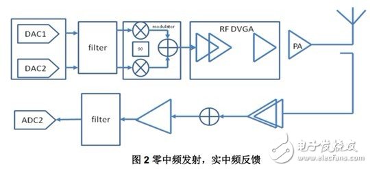
This solution is currently the most versatile architecture. Compared with architecture 1, the biggest difference is in the feedback channel, so its biggest advantage:
1) Since the transmission channel uses zero intermediate frequency, the system's local oscillator leakage and sideband calibration relative algorithm is relatively easy;
2) For the feedback channel, due to the digital high-IF method, the local oscillator leakage and image signal can be filtered by a simple filter without any calibration.
3) Due to the real IF scheme, only one feedback ADC is needed;
4) Reduced the sampling rate of the DAC, simplifying the anti-aliasing filter design between the DAC and the modulator (only a low-pass filter is required).
The disadvantages of this architecture are:
1) The ADC sampling rate of the feedback channel is very high, especially for TD-LTE 190MHz bandwidth requirements;
2) The filter of the feedback channel introduces the problem of DPD signal unevenness;
3) Two local oscillator signals are required. Most base stations currently use this architecture.
1.3 complex intermediate frequency transmission, complex intermediate frequency feedback
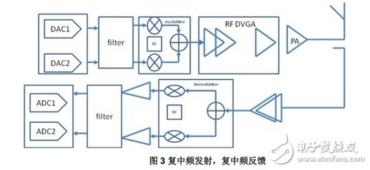
Compared with the scheme of FIG. 1, the difference is that the output signal of the DAC is a high intermediate frequency signal, and the input signal of the ADC is a high intermediate frequency signal, and the advantages are as follows:
1) The same local oscillator signal can be used for transmission and feedback, which simplifies system design and cost savings;
2) Local oscillator leakage and sideband suppression can be suppressed by filters, and the algorithm requirements are greatly reduced;
3) The low-order harmonic signal is out-of-band and can be suppressed by the filter, which reduces the requirements of the algorithm;
4) Due to the complex IF architecture, the adoption rate of the ADC of the feedback channel is reduced by half, especially for broadband TD-LTE systems.
Its disadvantages:
1) Since the signals of DAC and ADC are high frequency signals, their performance is relatively large;
2) The linearity of the demodulator will decrease;
3) The flatness performance of the transmit and feedback channels will be poor, which will have a relatively large impact on the performance of the DPD. Since DC and sideband calibration are not required, and the broadband signal can be easily supported, it is relatively large on TD-LTE. potential.
2. Analysis of TD-LTE transmitter indicators
This section introduces the air interface indicator requirements of TD-LTE and the corresponding system indicator allocation. According to 3GPP TS 36.104 requirements, the TDLTE air interface indicator requirements include: base station output power, base station output power dynamic range; transmitter on/off power; Machine signal quality; unwanted emission; launch intermodulation and others, the following will be analyzed and decomposed for important indicators.
2.1 Base station output power
The output power of the base station refers to the average power per carrier of the antenna port. This indicator requirement is usually proposed by the operator. Currently, TD-LTE usually requires 8 antennas with a maximum power output of 20W (43dBm). 3GPP requires accuracy. +/-2dB, guaranteed accuracy of +/-2.5dB under extreme conditions, but in order to simplify the power amplifier design, and good thermal design, the link guarantees power fluctuations of +/-1dB, in broadband signals, especially in China. The TD-LTE 190MHz bandwidth, how to ensure that the link power fluctuations within +/-1dB.
When selecting a link device, it is necessary to ensure that the power fluctuation in the 190MHz band is as small as possible, and the power fluctuation usually allocated to the DAC and the modulation is within +/-0.5dB. Currently, TI's DAC34H8X+TRF3705 can guarantee +/-0.5dB. In-band fluctuation requirements.
In addition to the choice of link devices to ensure better fluctuations, closed-loop power calibration is also necessary. The following table is an example of the requirements for closed-loop calibration.

2.2 Transmitter on/off power
The transmitter switch is an indicator requirement for TD-LTE. Since TD-LTE adopts the same frequency receiving/transmitting, the influence of the noise floor on the receiver is controlled within a certain range after the transmitting mechanism is disconnected. 3GPP requires it to After shutdown, the power is lower than -85dBm/MHz, after normalization: -85dBm/MHz=-(85+10*lg10^6)=-145dBm/Hz, the noise floor is allocated to the DAC modulator considering the gain. To ensure -155dBm / Hz or so.
2.3 Transmitter signal quality
The signal quality of the transmitter includes: frequency error; EVM (vector amplitude error); delay synchronization between multiple antennas.
2.3.1 Frequency error
3GPP requires that the frequency deviation observed by the modulated carrier frequency within one subframe period (1ms) must not exceed +/-0.05ppm. In TD-LTE transmitter systems, since the baseband system is fully synchronized and has no long-term frequency error, The frequency error is mainly due to the contribution of the clock and the frequency synthesizer.
2.3.2 EVM (Vector Amplitude Error)
The requirements of the 3GPP requirements for various modulated signals are as follows, and it is usually necessary for the designer to reserve a margin of 2-3%.

The contribution of EVM is mainly from several parts of the whole transmission: digital processing and link part.
1: CFR (peak clipping), in order to improve the efficiency of PA, peak clipping is the most important technology in combination with DPD. It has a very important impact on the EVM of the system. Different peak clipping techniques have different performances. The usual hard clipping summit It is relatively simple, but the impact on the system, especially on EVM, will be relatively large. At present, the commonly used method is the peak cancellation method. Although the required resources are more, it is optimal for the overall system performance. The impact of specific CFR on EVM, but it is important to understand that CFR has a very important impact on EVM.
2: link part
As shown in the following general diagram of the transmit link, we can list seven factors that affect EVM. This paper does not make a detailed derivation and directly applies the conclusion (2).

A: I/Q path is unbalanced, setting the gain difference to δ dB
in case 
Then you can get the following relationship between EVM and gain error.

B: Influence of phase shift error of quadrature modulator on β-to-EVM

C: Local oscillator leakage £ Impact on EVM

D: Local oscillator phase noise? Impact on EVM
Let G? be the power spectral density of phase noise, then

In addition to the above main effects, the amplitude-frequency characteristics of the channel filter are distorted, the nonlinear phase distortion of the channel filter, and the nonlinear distortion of the link affect the EVM of the transmitter. Equation (5) gives the calculation formula of the total EVM of the link.

2.3.3 Multi-antenna synchronization delay error
TD-LTE In addition to the phase requirements between multiple antennas required by smart antennas, the phase error between 3GPP and multi-antenna is also required to be no more than 65 ns. The delay usually assigned to the transmitter signal link must not exceed 30 ns, so the transmission is The link usually requires the modulator to have a common local oscillator, the DAC has a common clock, and because the FIFO is integrated in the DAC, the DAC is usually required to be synchronized, and if the phase delay between multiple antennas is fixed, compensation is usually required if multiple antennas There is uncertainty in the phase delay between them, and it is necessary to ensure that the uncertainty is as small as possible.
2.4 Un-wanted emissions
Un-wanted emissions include both out-of-band and stray radiation. Out-of-band radiation refers to the radiation requirements within the range from the lower limit of the transmitter's operating bandwidth to within 10 MHz, and the radiation requirements within 10 MHz above the upper limit. In the UMTS column, the transmitter operates at a bandwidth of 2110-2170 MHz, so out-of-band spurs refer to spur requirements in the range of 2100-2110 MHz and 2170-2180 MHz; signals in the frequency range except for the out-of-band radiation requirements, others The spurs in the area are attributed to the requirements of the stray radiation indicator.
2.4.1 Operating band unwanted emissions
Operating band unwanted emissions is one of the Un-wanted emissions. The contribution of the near-end is mainly due to the residual nonlinear products of the power amplifier after the DPD and the phase noise of the local oscillator signal. The contribution of the far-end is mainly due to the transmitting link. The noise floor, as well as the residual nonlinear products of the DPD rear power amplifier, the spurious to the far-end radiation of the launch link falling in the band also has a relatively large impact.
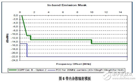
As shown above, the in-band spurious template, where blue is the FCC requirement, needs to meet 22dBm/MHz at 1MHz offset, while China Mobile only needs to meet the requirements of 3GPP cat A, and needs to meet the offset at 1MHz. -11dBm/MHz requirement, but in order to support beam forming, it needs to increase the requirement of 9dB, that is, when offsetting 1MHz, it needs to meet the requirement of -20dBm/MHz, set the power output of the power amplifier to 20W (43dBm), and the TD-LTE for 20MHz. In terms of signals, in order to meet 3GPP requirements.
0-1MHz: 43dBm-10*log (18MHz)-(-11dBm/MHz) =40.5dBc
1MHz-10MHz: 43dBm-10*log (18MHz)-(-13dBm/MHz) = 42.5dBc
10MHz: 43dBm-10*log (18MHz)-(--15dBm/MHz) = 44.5dBc
According to the above results, it can be assigned to each stage of DUC, CFR, modulator, power amplifier, etc., to ensure that the cascaded result must not be lower than the above values.
2.4 .2 ACLR (adjacent channel leakage power suppression ratio)
ACLR refers to the ratio of the mean power of the main signal to the power of the pilot signal. Generally, 3GPP cat A requires that it can satisfy the relative ratio of -45dB, or take the lead power of -13dBm/MHz as the absolute value. Take it lightly; cat B can be light in relative 45dB or absolute -15dBm/MHz, and the ACPR requirement is lower than the in-band spur requirement, which is usually used to evaluate the nonlinearity of the transmitter system. In the system, the PA driver, the nonlinearity of the modulation, the phase noise of the local oscillator signal, and the nonlinearity of the DAC all affect the ACLR of the system.
ACLR is a system indicator, the corresponding PA driver, the nonlinear index of the modulator is OIP3, and the rough conversion can be expressed as:
1 carrier ACPR=IIM3I-3dB
2 carrier ACPR=IIM3I-9dB
4 carrier ACPR=IIM3I-12dB
Therefore, OIP3 can be calculated from IM3, so that the OIP3 requirement for each level of device can be calculated according to the cascading formula of OIP3.
2.4.3 Transmitter spurious emissions
The transmitted spur refers to the 9KHz to 12.5GHz frequency band, and the spurious requirements in all frequency ranges except the in-band spurs are a mandatory requirement. The general spur indicators are summarized as follows, and the transmitting channel is different from the receiving channel. Scatter requirements, coexistence of spurs, co-sites and other spur indicators, for coexistence, the common site does not list all the frequency ranges, only some representative parts are listed, the specific design needs to be compared with all listed in 3GPP Spurious metric requirements for the frequency range.
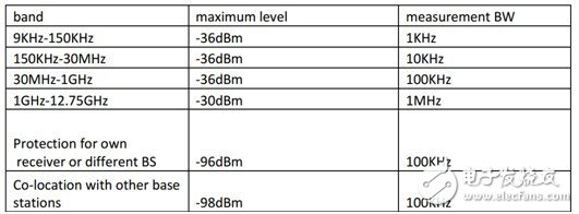
Especially for the signal interference of the receiver, it is necessary to ensure -96dBm-10*log(100KHz/Hz)=-146dBm/Hz, which is not filtered by the filter, and it is necessary to ensure that the output power is extremely low after the transmitting mechanism is broken; For the -98dBm spur requirement of the common site, it is necessary to suppress the corresponding co-site frequency when designing the duplexer.
Also consider that various possible intermodulation products fall within the corresponding frequency range (there are many tools for calculating intermodulation), taking into account various possible signals such as clock frequency and harmonics, PLL frequency and harmonics, and The intermodulation products between them.
2.4.4 Transmitting intermodulation
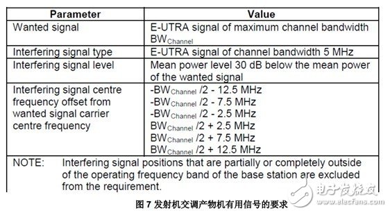
The transmit intermodulation requirement is used to test the transmitter's ability to suppress its own nonlinearity. The interfering signal is 5MHz E-UTRA, and the average power is 43dBm-30dB=13dBm. The position is located at +/-12.5MHz from the main signal. , +/- 7.5 MH at +/- 2.5 MHz, the intermodulation product should meet the stray radiation template of Figure 6.
3. TI TD-LTE transmission key device requirements
The second section analyzes the transmitter's index requirements in detail. This section will introduce the requirements of key devices (DAC+ modulator, clock, frequency synthesis) according to its specifications and TI's solution.
3.1 DAC+ modulator
High bandwidth: Supports 190MHz BW, requires a DPD bandwidth of at least 600MHz, and a DAC data rate of 750MHz.
(750*0.8=600MHz) DAC sampling rate 750*2=1.5Gpbs, DAC34SH84 sampling rate 1.5GHz, supporting up to 600MHz signal bandwidth.
Low noise: Considering the far-end noise mask requirement, retaining 13dB margin, the noise requirement of DAC+ modulation should be lower than: -22dBm/MHz-13dB-(-43dBm-(-14dBm))-10lg1MHz=-152dBm/Hz, DAC34SH84 noise The bottom is -156dBm/Hz, and the TRF3705 noise floor is -157dBm/Hz, so the total noise is about -153dBm/Hz.
Flatness: Figure 8 shows the flatness of the DAC34SH84+TRF3705, combined with frequency calibration to meet flatness requirements.
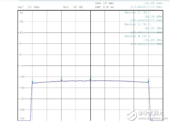
Figure 8 DAC34SH84+TRF3705 flatness
SFDR: Consider single-carrier signal, bandwidth 20MHz, for in-band spur indicator requirements, assuming 10% contribution from DAC34SH84+TRF3705, SFDR needs to be better than: [43dBm-10lg (18MHz)]-[(-22dBm)-(10lg1MHz )]-10lg0.1=63dB
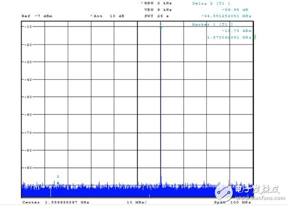
Figure 9 DAC34SH84+TRF3705 SFDR
to sum up
This paper introduces the system requirements and decomposition of the transmitter in detail, the requirements of various indicators on the system, and the selection of key devices. Combined with TI's solution DAC34SH84+TRF3705, it provides a set of solutions for transmitter system analysis for TD-LTE. And the basis for device selection.
Touch Panel For Iphone,Touch Screen Digitizer Panel,Touch Screen Panel For Iphone,Phone Touch Screen
Shenzhen Xiangying touch photoelectric co., ltd. , https://www.starstpmobile.com