In high-speed digital circuit design, the influence of parasitic capacitance and inductance of vias cannot be ignored. At this time, the vias appear as discontinuous breakpoints in the transmission path, which will generate signal integrity such as reflection, delay, and attenuation of signals. problem. In this paper, the effects of via length, via aperture, and pad/anti-pad diameter on via impedance are investigated using a vector network analyzer. By adding a grounding hole beside the signal hole, a loop method is provided for the via current, which improves the continuity of the via impedance and effectively reduces the via loss. The results show that the increase of the grounding hole can control the impedance of the via hole. The impedance of the via hole decreases with the increase of the number of grounding holes. When four grounding holes are used, the impedance of the via hole can be approximated by the impedance formula of the coaxial cable. In addition, the paper also discusses the effect of excess stubs on vias on via impedance and loss. The results show that for every 0.10 mm increase in the excess stub length of the via, the via resistance decreases by 0.4-0.9 ohm, and the via loss increases as the length of the excess stub increases. This study can provide a basis for the design and optimization of high-speed digital circuit vias.
1 IntroductionIn modern high-speed digital circuit design, the influence of vias on PCB signal integrity cannot be ignored [1-2]. Multi-layer PCBs are often used in high-speed designs. In multi-layer boards, signals are transmitted from one layer of interconnect to another, and via vias are required to connect. At frequencies below 1 GHz, The hole can play a good connection, and its parasitic capacitance and inductance can be neglected. When the frequency is higher than 1 GHz, the influence of the parasitic effect of the via on the signal integrity cannot be ignored. At this time, the via appears as a discontinuous breakpoint in the transmission path, which will cause signal reflection, delay, attenuation, etc. Signal integrity issues [3]. When the signal is transmitted to another layer through the via, the reference layer of the signal line also serves as the return path of the via signal, and the return current flows between the reference layers through capacitive coupling, causing problems such as ground bounce [4-5 ].
At present, there are few reports on the related research on vias, and the research basically uses simulation software to simulate the influence of via parameters on via impedance and S parameters [6-8]. These simulation results can only help the designer to understand the influence of the relevant parameters on the via impedance and signal integrity, but can not accurately give the degree of influence of the via parameters, and it is difficult to guide the actual engineering design. In this study, the single-ended via impedance was studied by using the network analyzer to test the TDR curve method. The effects of via aperture, via length, and pad/anti-pad size on the via impedance were analyzed. By providing a return for the via signal. The path method is used to study the influence of grounding holes on the impedance and loss of vias. The influence of excess short columns on the impedance and loss of vias is also discussed.
2, test methods2.1, main materials and instruments
Material: FR4 copper clad with different thickness, copper thickness 1/1 OZ; prepreg (106, 1080, 2116 and 3313).
Instrument: Vector Network Analyzer (VNA) with a bandwidth of 20 GHz.
2.2, method
Different layer test boards were fabricated, the signal via hole design value was 0.20-0.50 mm, and the via length was designed to be 0.5-2.0 mm. Different size pads and anti-pads were designed. In order to study the influence of excess short column on the impedance and loss of the via hole, the test obtained the single-ended via of different short column length by back-drilling technology and controlled back-drilling depth. The length of the via hole was 0.20-0.80 mm.
Test board production process: material opening → baking board → inner layer dry film → inner layer etching → inner AOI → browning → lamination → drilling → de-staining → copper sinking → outer plating → tin plating → back drilling → outside Layer etching→outer layer dry film→pattern plating→outer etching→external AOI→resistance welding→immersion gold→milling board...
After the test board is completed, the TDR curve and S-parameters of the single-ended line with vias are tested by a vector network analyzer. The resistance value of the TDR curve is obtained through the change of the TDR curve at the via hole, and the via loss is analyzed by the S parameter.
3. Results and discussion3.1. Effect of via parameters on impedance continuity
The via length is one of the main factors affecting the via inductance [1]. For vias used for top and bottom conduction, the via length is equal to the PCB thickness. Due to the increasing number of PCB layers, the PCB thickness often reaches more than 5 mm. However, in high-speed PCB design, to reduce the problems caused by vias, the via length is generally controlled within 2.0 mm. Here, the change in via resistance was observed when the via length was changed from 1.0 to 2.0 mm (see Figure 1). It can be seen from the figure that when the via length is increased from 1.0 mm to 2.0 mm, the via resistance increases rapidly due to the rapid increase of the via inductance, that is, the larger the via length, the worse the via resistance discontinuity. The test also shows that when the via length is in the range of 1.0 mm, the impedance variation caused by the via can be controlled within 10% by the optimization of the via parameters, but the via resistance discontinuity is obtained when the via length exceeds 1.5 mm. The problem has become difficult to solve.
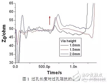
Figure 2 shows the effect of via aperture on via impedance. As can be seen, when the via aperture is increased from 0.20 mm to 0.50 mm, the via resistance is reduced from 58.4 ohms to 52.5 ohms. This is mainly due to the increase in via capacitance due to the increase in via aperture, which is inversely proportional to the capacitance. For vias with a via length greater than 2.0 mm, by increasing the via aperture, the via impedance continuity can be improved to some extent. When the via length is 1.0 mm or less, the optimum via hole diameter is 0.20-0.30 mm.
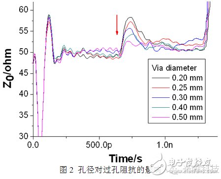
Figure 3 shows the effect of via pad size on via impedance. As can be seen from the figure, when the via pad diameter is increased from 0.45 mm to 0.55 mm, the via resistance is reduced from 57.5 ohms to 55.2 ohms. This is due to the increased size of the via pad, which also results in an increase in via capacitance. From the test results, it can be concluded that for every 0.05 mm increase in via pad size, the via resistance drops by about 0.5-0.7 ohm.
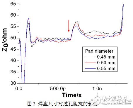
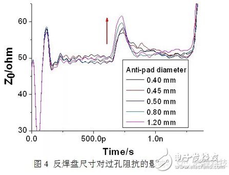
Figure 4 shows the effect of the anti-pad size on the via impedance. As can be seen from the figure, when the anti-pad size is increased from 0.40 mm to 1.2 mm, the via resistance increases from 57.1 ohms to 61.7 ohms. This shows that by optimizing the size of the via anti-pad, it is also possible to improve the continuity of the via resistance.
3.2. Influence of grounding holes on via impedance and loss
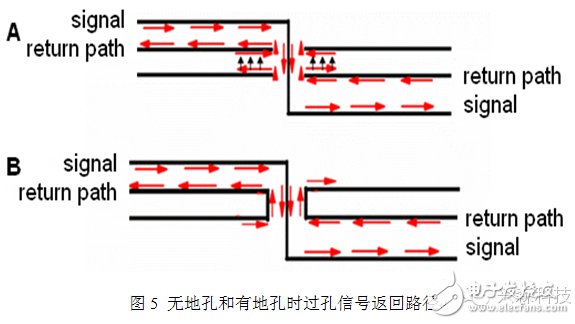
For a 4-layer board, two things can happen when the signal is transferred from the top-level transmission line to the bottom layer (see Figure 5). Figure 5 (A) shows the case where there is no hole near the signal via. When the signal passes through the via, the return path returns through the two layers. The uncontrolled return current produces a ground bounce effect, and the signal is generated when passing through the via. Electromagnetic waves (EM) are transmitted on both bottom layers, causing voltage fluctuations that cause signal integrity problems [9-10]. Figure 5 (B) shows the increase of the grounding hole. At this time, the grounding hole provides a complete return path for the via signal, and also provides a reference hole for the via signal, thereby improving the impedance continuity of the signal via and reducing Small signal loss. Here we mainly study the influence of the grounding hole on the impedance and loss of the via.
In the test, 1 to 4 grounding hole reference holes were added next to the single-ended signal vias. The influence of the number of grounding holes on the impedance of the single-ended vias was investigated. The results are shown in Fig. 6. As seen from the figure, the via impedance decreases as the number of ground vias increases. This is because the capacitance between the signal via and the ground hole increases as the number of ground holes increases, that is, the number of ground holes can be adjusted to effectively control the via impedance.
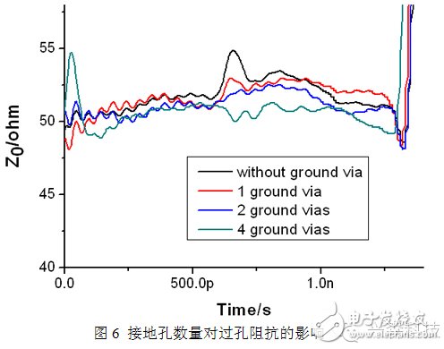
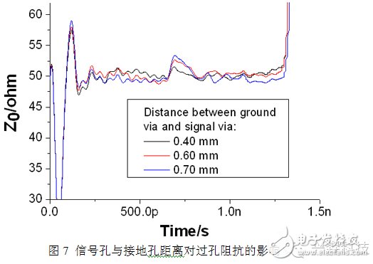
Figure 7 shows the effect of the distance between the signal hole and the ground hole on the impedance of the via. It can be seen from the figure that when the distance between the signal hole and the ground hole increases from 0.40 mm to 0.70 mm, the impedance of the via hole increases continuously. Similar to the transmission line with the ground layer as the reference layer, after the grounding hole is added, the signal via hole uses the grounding hole as the reference hole. When the distance between the signal hole and the ground hole increases, the capacitance between the signal hole and the ground hole decreases, and the impedance of the via increases. It can be seen that the impedance of the via hole can be controlled by adjusting the distance between the signal hole and the ground hole.
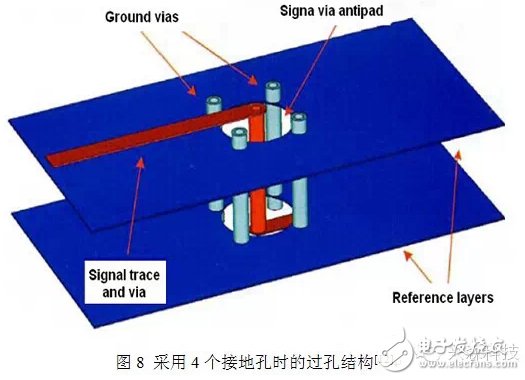
Through the above test, it can be found that when there are four grounding holes around the signal hole (see Figure 8 for the effect), the structure is similar to that of the coaxial cable. At this time, the single-ended via impedance can be approximated by the coaxial cable impedance formula (Equation 1) [11].

Where D represents the diagonal distance of the ground reference hole, d represents the aperture of the signal hole, and ε is the dielectric constant of the dielectric layer.
The via resistance at different design parameters can be calculated by equation (1). The results are shown in Table 1. It can be seen from the table that the theoretical calculation of the via impedance is basically consistent with the measurement results. This indicates that the via impedance of the via of the structure can be approximated using the coaxial cable impedance equation.
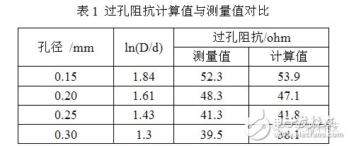
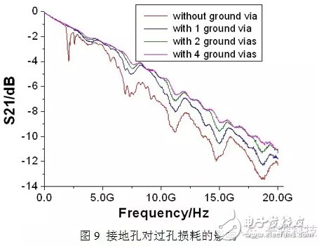
Figure 9 shows the effect of ground vias and number on via loss when the via hole diameter is 0.20 mm and the via length is 1.0 mm. It can be seen from the figure that after the grounding hole is increased, the via loss is significantly reduced, and the more the number of the grounding holes, the smaller the via loss. This is because the ground reference hole provides a complete return path for the via signal, which significantly reduces the impedance discontinuity caused by the via, and the signal reflection caused by the discontinuity of the impedance is weakened, so the via loss is reduced. After the grounding hole is added, the crosstalk between the signal vias can be weakened, and the quality of the via signal transmission can be improved. At the same time, the grounding hole can also avoid EMC/EMI problems caused by radiation [4].
3.3 Effect of excess short column on via impedance and loss
In high-speed multi-layer PCBs, when a signal is transmitted from the top layer to a certain internal layer, the via connection creates extra via stubs, which greatly affect the signal transmission quality. When the signal is transmitted through the via to another layer of impedance matching, a portion of the energy is transferred to the stub of the via, and this portion can be considered as a fully open state due to the absence of any impedance termination. Therefore, this branch will cause total reflection of the remaining energy, which greatly weakens the signal quality and damages the integrity of the original signal [1]. The use of blind holes and buried holes can effectively avoid the influence of short columns on signal integrity, but the technology is complicated and costly. The back-drilling technique is used to drill out the excess short column in the signal hole to obtain better transmission quality of the via signal. Therefore, studying the influence of the short column on the signal integrity of the via hole helps to balance cost and performance.
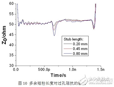
In order to study the influence of short columns on the signal integrity of the vias, the test obtained single-ended vias with different short column lengths by using back-drilling technology and controlling the back-drilling depth method. Figure 10 shows the effect of the excess stub length on the via impedance. It can be seen from the figure that when the length of the extra short column increases from 0.20 mm to 0.80 mm, the via resistance decreases continuously; for every 0.10 mm increase of the excess short column length, the via resistance decreases by about 0.40-0.90 ohm.
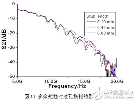
The effect of extra short columns on via loss is also studied here. Figure 11 shows the change in via loss when the excess stub length of the via increases from 0.20 mm to 0.80 mm. It can be seen from the figure that with the increase of the length of the extra short column, the via loss shows a significant increase trend, and the longer the short column, the larger the resonance amplitude; at the 10 GHz frequency, the excess short column length increases by 0.10 mm, and the via loss increases by 0.15. dB. The test also shows that the larger the signal via hole diameter, the greater the influence of the excess short column on the via resistance and loss.
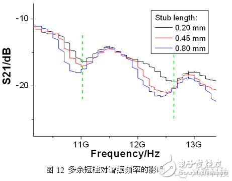
The extra short column will cause the capacitance of the via to increase, and the larger the length of the short column, the higher the capacitance, and the increase of the capacitance will cause the resonance frequency to decrease, so that the loss near the resonance point becomes larger. The relationship between resonant frequency and capacitance and inductance can be described by equation (2). Figure 12 shows the resonance for different short column lengths. It can be seen from the figure that the longer the excess short column, the lower the resonance frequency. When the lengths of the short columns are 0.20 mm, 0.45 mm and 0.80 mm, respectively, the second resonant frequencies of the vias are 11.03 GHz, 10.99 GHz, 10.92 GHz, respectively, and the third resonant frequencies are 12.66 GHz, 12.52 GHz and 12.39 GHz, respectively.

By optimizing the via design aperture, via length, and pad/anti-pad size, the via impedance continuity is effectively improved. When the via length is less than 1.0 mm, the four design parameters can be optimized to control the impedance variation caused by the vias to within 10%. Providing a return path for the via signal allows control of the via impedance and reduces the signal loss of the via. When using four ground reference holes, the via impedance can be approximated by the coaxial cable impedance equation. Excess short columns can result in reduced via resistance and increased losses.
Car Phone Holder,Mobile Holder For Cars,Mobile Phone Holder For Dashboard,Mobile Phone Holder For Car Dashboard
Ningbo Luke Automotive Supplies Ltd. , https://www.nbluke.com