The concept of LED enterprises in China is gradually changing. More and more small and medium-sized enterprises have begun to deploy strategically. They gradually attach importance to the accumulation of intellectual property in the early stage, learn to use science and technology to arm themselves, and use patents to develop domestic and foreign markets. The trap has become a good market prospect. With a good experimental field and a breakthrough direction, companies should learn more lessons so that they can fly higher and further.
It is understood that China's LED industry is still facing a series of urgent problems to be solved, including the uneven quality of products, the price war is still very serious, the sales channel thinking is still relatively conservative, and the effective resources have not been fully utilized. Based on the current severe price war, many companies are frightened, but in contrast, the price war has been improved in the industrial chain, and the product cost has been effectively controlled.
In order to usher in the harvest of autumn, we must finally look at the wisdom of the company itself. Smart companies should look up to international competition, no longer indulge in the "infighting" around them, and seek long-term development of "strong alliance", identify their position in the industrial chain, and concentrate on building core competitiveness. .
The central bank cut interest rates, the real estate industry is generally rejoicing, that house prices will likely usher in a rebound. Of course, not all city prices will rebound. So how big is the impact on the LED industry, including the four first-tier cities in the north, Guangzhou and Shenzhen, and Xiamen and Nanjing, which are the most likely to rebound in housing prices.
The possibility of a significant volume and price Qi Zhang industry has brought substantial positive <br> <br> central bank released the news: cut financial institutions RMB benchmark deposit and lending rates, one-year benchmark lending interest rate by 0.4 percentage points to 5.6%; The one-year deposit benchmark interest rate was lowered by 0.25 percentage points to 2.75%; the benchmark interest rate for loans over 5 years was 6.15% (previously 6.55%), and the interest rates of other grades were adjusted accordingly. According to market analysis, this interest rate cut is definitely good for the property market.
The interest rate cut will be a substantial positive for the manufacturing industry, especially for the LED industry, which faces a decline in exports and a slowdown in domestic demand. This move will undoubtedly create new opportunities for industrial development in the future market. In the capital market, continuous interest rate cuts and deposit reserve ratios must release huge liquidity, and liquidity has completely bid farewell to the tightening situation and usher in an upward turning point. While reducing the risk-free rate of return, it will also raise the equity risk premium and enhance the attractiveness of the LED listed company's stock market relative to other investment products. Most of the manufacturing industries, including LED companies, will be the beneficiaries of this profit pattern adjustment. Lowering the loan interest rate will reduce its borrowing costs, reduce the financial expenses to the erosion of profits, and boost the profitability of enterprises. In the case of manufacturing, it will solve the great difficulties of enterprises. This determines that the more sensitive the profit is to the cost of borrowing, the more the industry can enjoy the benefits of this rate cut cycle.
In the current global economic slowdown, both large enterprises and small and medium-sized enterprises are hoping to reduce costs, especially for capital-intensive manufacturing companies, and the most direct effect of interest rate cuts is to reduce corporate capital costs.
Industry may still face a slowdown <br> <br> pressure from the LED report for further expansion of domestic demand in the country, driven by investment policy trillion, driven by a large number of infrastructure for the project type LED business opportunities and challenges The current round of interest rate cuts has just begun. After several interest rate cuts, the current benchmark deposit rate has fallen. Analysts pointed out that this shows that the current economy has cooled significantly. As the outlook for the future economic situation is still not optimistic, domestic consumption and industrial production growth may continue to decline. Analysts said that in terms of time and scope, the current round of interest rate cuts has not been more than half, and the stimulus for economic growth is still to be observed. For the entire LED industry, it may still face pressure to slow down.
Accelerate innovation and promote development <br> <br> under the influence of the international financial crisis, China's LED business part of the production and operation difficulties encountered in economic good times, some companies may lack vision and motivation of independent innovation, and to the "Extreme time", the huge demonstration effect of independent innovation immediately appeared, and enterprises that do not attach importance to independent innovation will be "forced" on the road of independent innovation, otherwise the road will become narrower and narrower.
At the same time, we will continue to deepen the cooperation between industry, universities and research institutes, strengthen technical cooperation with scientific research units, strengthen scientific and technological support, and smoothly realize transformation and upgrading. The main body of independent innovation is the enterprise, and the ultimate beneficiary is also the enterprise. The key to increasing investment in scientific research and development is to work hard on irreplaceability.
Seek cost-effective way to expand <br> <br> plight of the financial crisis in LED applications, the small and medium manufacturing enterprises are facing not just rely on a single tool or measures will be able to save the. He also needs the company's own plan and determination to get out of trouble, and needs the policy support of the government. Low-cost and efficient marketing targeting of target consumers is a more sensible choice. Relying on the network, attach importance to e-commerce, reduce the promotion costs of enterprise products, and seek high-efficiency and low-cost expansion methods to embark a new path during the economic downturn.

8 Layer PCB - Stackup & Cost & Prototype manufacture
What is 8 layer PCB?
The 8 layer PCB is a circuit board with 8 layers that are stacked firmly together with predefined and dependable mutual connections between the layers. Structure of eight layer PCB is more complicated. Nowadays, PCBs frequently have 8 to 12 layers or more, and electronics engineers know that designing for so many layers requires a well-configured layer stack.
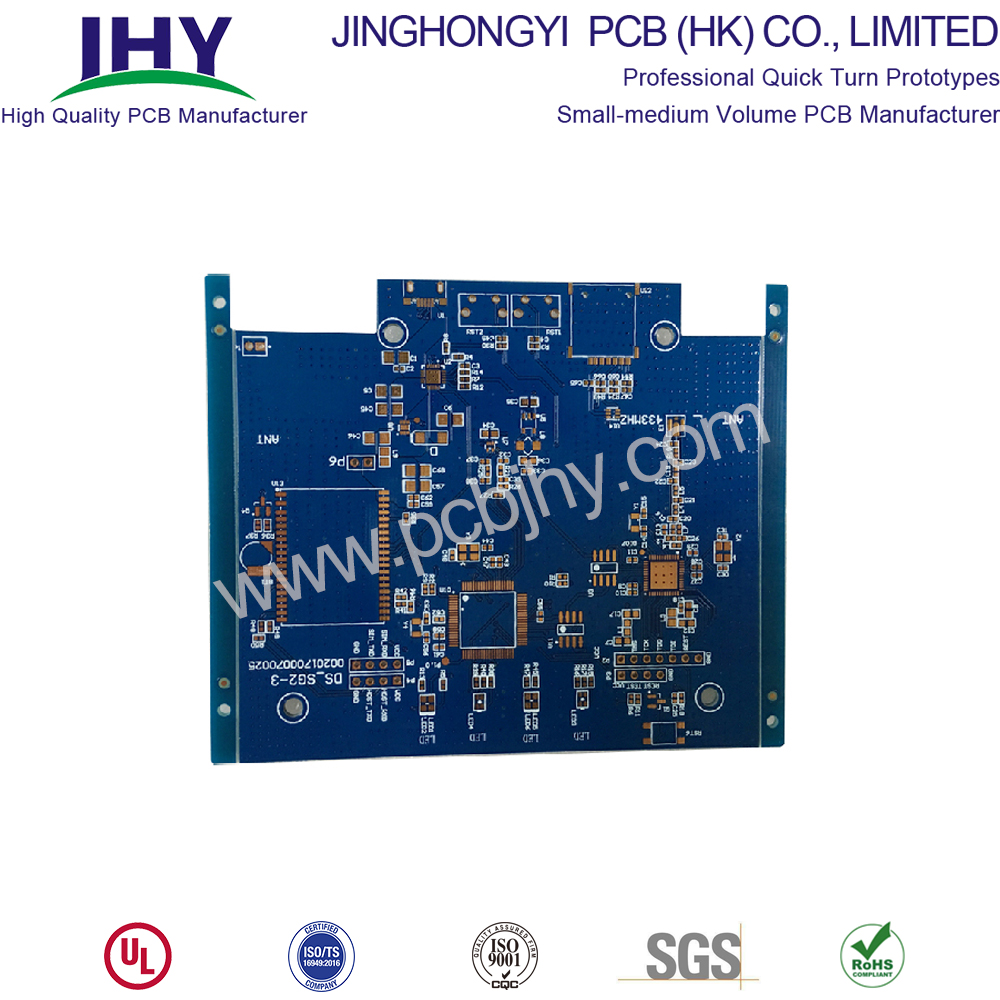
8-layer Printed Circuit Boards are usually installed in compact equipment with strict spacing requirements, such as notebook computer motherboard, communication backplane, wearable watches, etc. Because of its complexity and high manufacturing costs, your 8-layer PCB Manufacturing should be made by reliable and experienced manufacturers. Jinghongyi PCB has been specially targeting high-end PCB manufacturing and assembly services for 8 years, providing high-quality products and services for various customers. Our advanced production line and fast response team will keep you comfortable and reassured, without any trouble, you can rest assured to place the order with us.
Typical 8-layer PCB stack up methods and guidelines
Standard stackup of 8 layer PCB looks as follows
- Signal1
- Ground
- Signal2
- Power
- Ground
- Signal3
- Power
- Signal4
Eight-layer PCB can be used to add two additional layers, or two planes can be added to improve EMC performance. Most eight-layer circuit boards are superimposed to improve EMC performance, rather than adding additional wiring layers. Compared with 6-layer circuit boards, the cost increase percentage of 8-layer PCB is less than that of 4-layer PCB to 6-layer PCB. Therefore, in order to improve EMC performance, the cost increase is reasonable. Therefore, most 8-layer boards consist of four wiring layers and four planes.
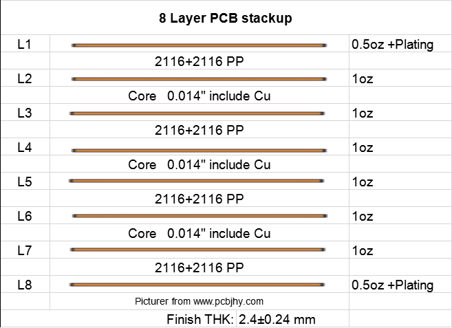
8 Layer PCB Stack up
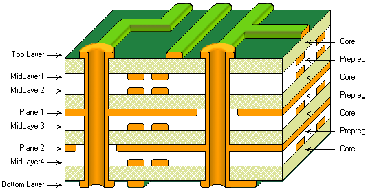
8 Layer PCB stackup
In short, 8 layer PCB are usually used to improve the EMC performance of circuit boards, rather than increasing the number of layers.
No matter how you decide on the stack layer, it is not recommended to use an 8-layer PCB Board with six wiring layers. If you need six routing layers, you should use a 10 Layer PCB board. Therefore, the 8-layer board can be regarded as the six-layer board with the best EMC performance.
Basic Layer of Eight-Layer Circuit Board with Excellent EMC Performance
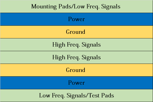
All signal layers are adjacent to the plane, and all layers are tightly coupled. High-speed signals are buried between planes, so planes provide shielding to reduce the transmission of these signals. In addition, the circuit board uses multiple grounding layers to reduce the grounding impedance.
Other forms of 8-layer PCB stackup
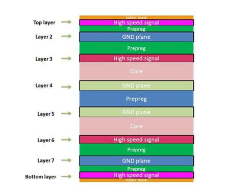
A typical 8 Layer PCB Stackup
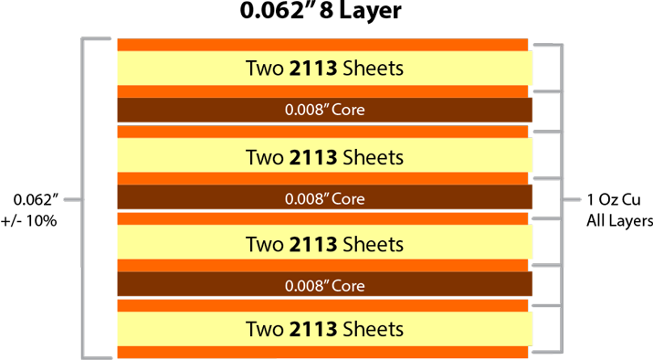
0.062[8 layer PCB stackup
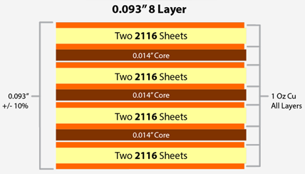
0.093[ 8-Layer PCB Stackup
So far, we have also clarified the cost and price differences between 6-layer PCB, 8-layer PCB and 10-layer PCB.
8 Layer PCB thickness
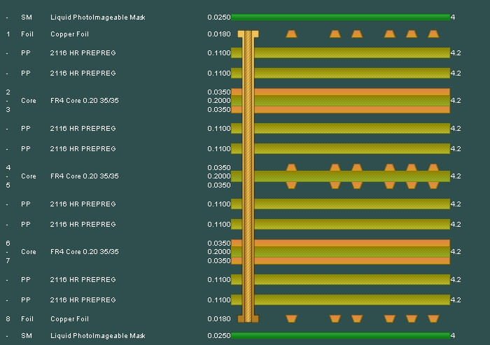
8 LAYER 1.6 MM STANDARD STACKUP AND THICKNESS
8 Layer Stackup - 1.6mm thickness |
||||||
| layer order | layer name | material type | material description | dielectric constant | thickness | copper weight |
| 1 | top | copper | signal | 0.035mm | 1 oz | |
| 2116 | prepreg | 4.5 | 0.12mm | |||
| 2 | inner 1 | copper | plane | 1 oz | ||
| core | 4.6 | 0.3mm | ||||
| 3 | inner 2 | copper | plane | 1 oz | ||
| 7630 | prepreg | 4.7 | 0.2mm | |||
| 4 | inner 3 | copper | plane | 1 oz | ||
| core | 4.6 | 0.3mm | ||||
| 5 | inner 4 | copper | plane | 1 oz | ||
| 7630 | prepreg | 4.7 | 0.2mm | |||
| 6 | inner 5 | copper | plane | 1 oz | ||
| core | 4.6 | 0.3mm | ||||
| 7 | inner 5 | copper | plane | 1 oz | ||
| 2116 | prepreg | 4.5 | 0.12mm | |||
| 8 | bottom | copper | signal | 0.035mm | 1 oz | |
| Final board thickness: 1.6mm±0.13mm | ||||||
8-Layer Prototype PCB Manufacturing Service
The 8-layer prototype FR-4 PCB is an 8-layer circuit board, which is firmly stacked together with predefined and reliable interconnection between layers. The 8-layer FR-4 PCB has more complex structure. JHYPCB is a large enterprise located in Shenzhen, China, which can manufacture 8-layer prototype PCB.
JHYPCB can provide you with multi-layer PCB board in accordance with RoHS standard. With laminated material, it can match high temperature in assembly process. Importantly, some lead-free assembly processes will require laminated substrates to withstand temperatures exceeding 260 degrees Celsius or 500 degrees Fahrenheit over a longer period of time. To solve this problem, we have high temperature laminates in stock, so that our customers can meet the higher temperature cycle requirements of some lead-free assembly applications.
JHYPCB is one of the leading 8 layer PCB manufacturers. For more information, pls send email to us.
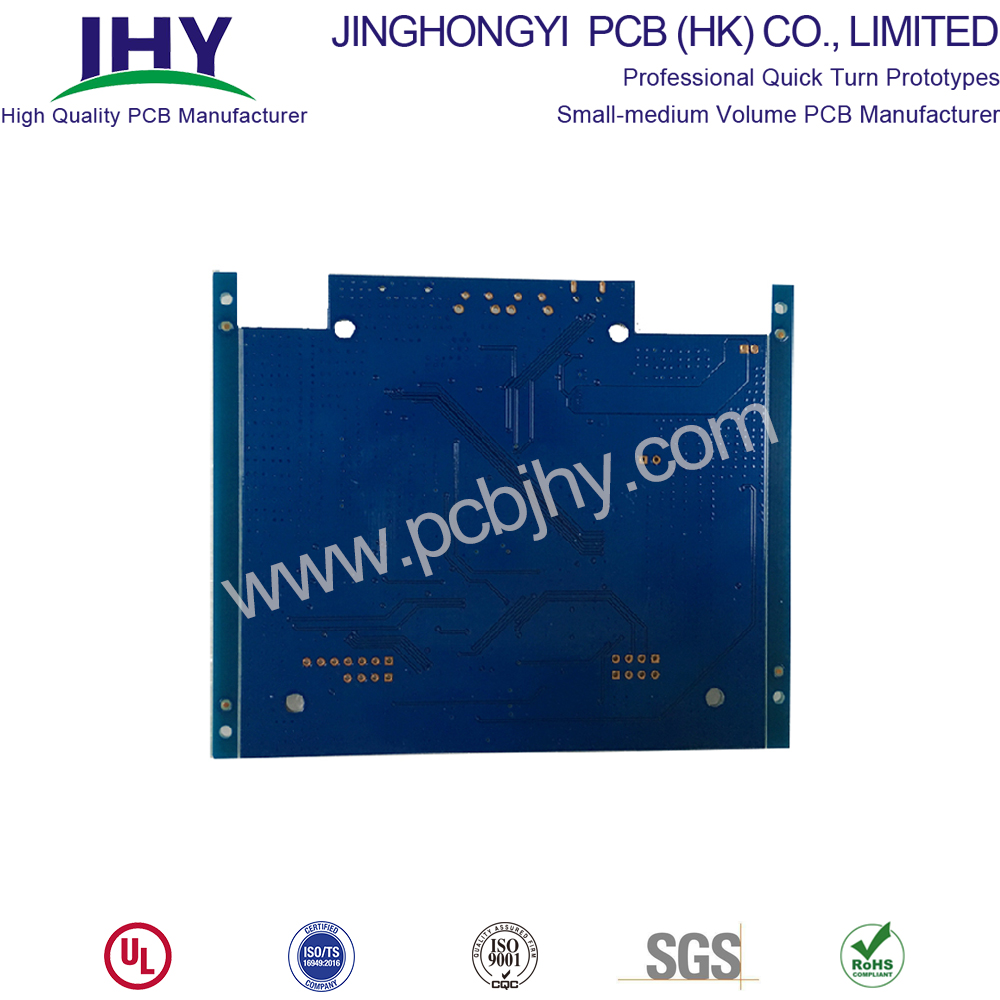
8 Layer PCB
PCB Circuit Board,8 Layer PCB,Custom multilayer pcb,Custom 8 Layer PCB
JingHongYi PCB (HK) Co., Limited , https://www.pcbjhy.com