As an energy conversion device operating in a switching state, the voltage and current change rate of the switching power supply is high, and the generated interference intensity is large; the interference source is mainly concentrated during the power switch and the heat sink and the high-level transformer connected thereto, with respect to the number The location of the circuit interference source is clear; the switching frequency is not high (from tens of kilohertz and several megahertz), the main form of interference is conducted interference and near-field interference; and printed circuit board (PCB) traces are usually hand-routed. It has greater randomness, which increases the difficulty of extracting PCB distribution parameters and estimating near-field interference.
The specific solutions for each frequency point are as follows:
Within 1MHz:
Differential mode interference is dominant 1. Increase X capacitance; 2. Add differential mode inductance; 3. Low power supply can be processed by PI filter (it is recommended to use larger electrolytic capacitors near the transformer).
1M-5MHz:
Differential mode common mode mixing, using input and a series of X capacitors to filter out the differential interference and analyze which interference is exceeded and solve;
5MHz:
The above is mainly based on common touch interference, and the method of suppressing common touch is adopted. For the grounding of the case, using a magnetic surround of 2 turns on the ground will have a greater attenuation of interference above 10MHZ (diudiu2006); for 25-30MHZ, it can be used to increase the capacitance of the ground Y and the copper skin outside the transformer. Change the PCBLAYOUT and the small magnetic ring wound in front of the output line with a minimum of 10 turns, at both ends of the output rectifier and RC filter.
1M-5MHZ:
Differential mode common mode mixing, using a series of X capacitors in parallel with the input terminal to filter out the differential interference and analyze which type of interference exceeds the standard and solve it. 1. For the differential mode interference exceeding the standard, the X capacitance can be adjusted, and the differential mode inductor can be added. , adjust the differential mode inductance; 2. For common mode interference exceeds the standard, add common mode inductance, choose reasonable inductance to suppress; 3. Can also change the characteristics of rectifier diode to handle a pair of fast diodes such as FR107 pair of common rectifier diode 1N4007 .
5MHz or more:
The common touch interference is mainly used to suppress the common touch.
For the grounding of the casing, 2-3 turns of a magnetic ring on the ground wire will have a greater attenuation effect on the interference above 10MHZ; the core-bonded copper foil close to the transformer can be selected, and the copper foil is closed. The size of the absorption circuit of the back-end output rectifier and the parallel capacitance of the primary large circuit are processed.
For 20M-30MHz:
1. For a class of products, you can adjust the Y2 capacitance to the ground or change the Y2 capacitor position;
2. Adjust the Y1 capacitor position and parameter value between the secondary side;
3. Bread copper foil outside the transformer; the innermost layer of the transformer is shielded; adjust the arrangement of the windings of the transformer.
4. Change the PCB Layout;
5. The output line is connected to a small common-mode inductor surrounded by a double line;
6. Connect the RC filter at both ends of the output rectifier and adjust the reasonable parameters. 7. Add BEADCORE between the transformer and the MOSFET. 8. Add a small capacitor to the input voltage of the transformer. 9. You can increase the MOS drive resistance.
30M-50MHz:
Generally, the MOS tube is turned on and off at high speed. It can be used to increase the MOS drive resistance. The RCD snubber circuit uses a 1N4007 slow tube, and the VCC supply voltage is solved with a 1N4007 slow tube.
2. The RCD buffer circuit uses a 1N4007 slow tube;
3. VCC supply voltage is solved by 1N4007 slow tube;
4. Or the front end of the output line is connected in series with a small common-mode inductor wound by two wires;
5. Connect a small snubber circuit in parallel with the DS pin of the MOSFET;
6. Add BEADCORE between the transformer and the MOSFET;
7. Add a small capacitor to the input voltage of the transformer;
8. PCB LAYOUT when the large electrolytic capacitor, transformer, MOS circuit loop is as small as possible;
9. The circuit loop formed by the transformer, output diode, and output smoothing electrolytic capacitor is as small as possible.
50M-100MHZ:
It is generally caused by the reverse recovery current of the output rectifier.
1. It is possible to string magnetic beads on the rectifier tube;
2. Adjust the absorption circuit parameters of the output rectifier;
3. It can change the impedance of the secondary capacitor across the Y-capacitor branch, such as adding BEADCORE at the PIN pin or connecting the appropriate resistor in series;
4. It is also possible to change the MOSFET, the output of the rectifier diode body to the space radiation (such as iron clip card MOSFET; iron clip card DIODE, change the ground point of the heat sink). 5. Increase the shielding copper foil to suppress radiation to the space.
100M-200MHz:
It is generally caused by the reverse recovery current of the output rectifier. It can be mostly between PFCMOSFET and PFC diode between the 100MHz-200MHz series of magnetic beads on the rectifier. Now the MOSFET and PFC diode string beads have effect, and the horizontal direction can basically solve the problem. But the vertical direction is very helpless.
The radiation of the switching power supply generally only affects the frequency band below 100M. It is also possible to add a corresponding absorption loop to the MOS and diode, but the efficiency will be reduced.
Above 200MHz:
The switching power supply has a basic amount of radiation and generally can pass the EMI standard.
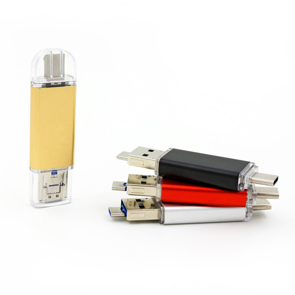
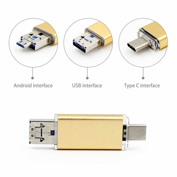
3 in 1 Custom Usb Flash Drive Type-C 8G 16G 32G 64G. Easy to transmit data between Micro-USB, USB and Type-C port devices, such as macbook, Type-c smartphone and tablet, Android smartphone and tablet, computuer and laptop. No need any adaptors, sharing data conveniently and save time.
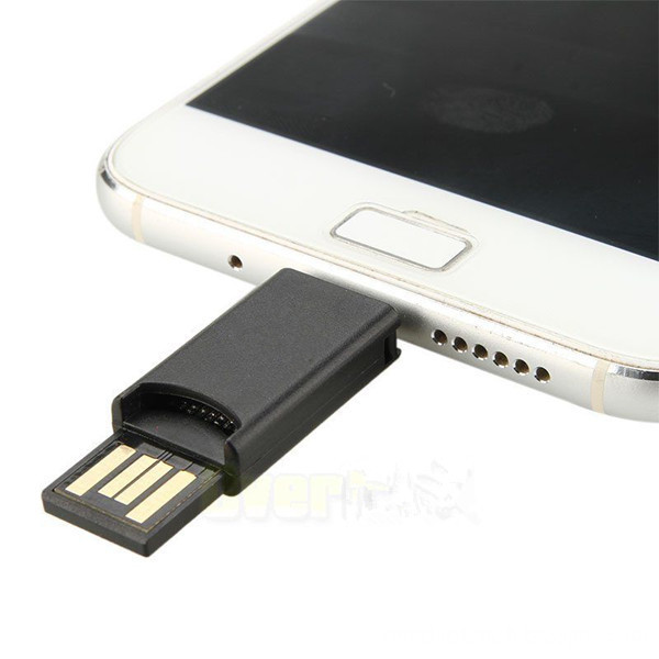
Black Type C Card Reader
This product is suitable for OTG-enabled Type-C interface phone. Easy to copy the memory card data to the phone, such as photos, video clips, office documents, etc. Support microSD, TF card. Can also be used directly to read U disk.
Type C Dual Port USB Flash Drive TF SD Card Reader
OTG supported. Read TF/SD card directly on your USB C , Micro USB OTG supported devices and other USB port device. Adding an memory card, turns your card reader into a U Flash Disk. Aluminum Shell.Slim,light and fashion design, portable and convenient for using. 3 in 1 : Compatible with USB C device,Micro USB OTG supported devices and USB port device.
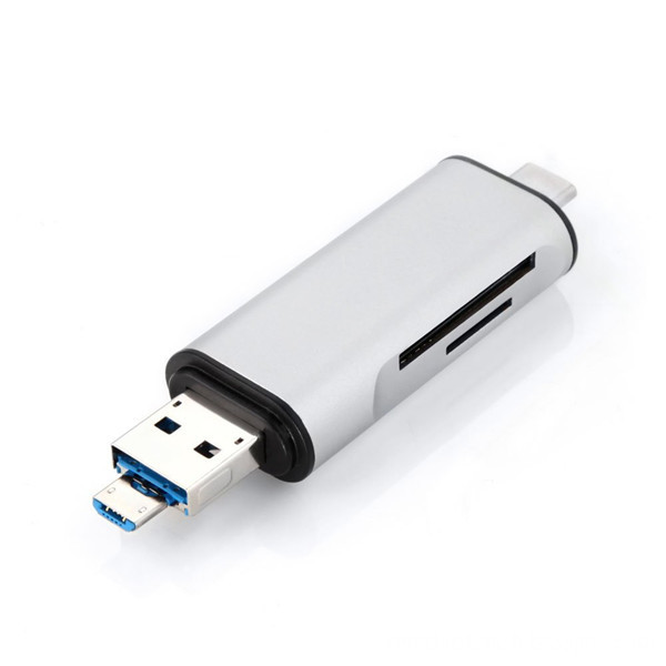
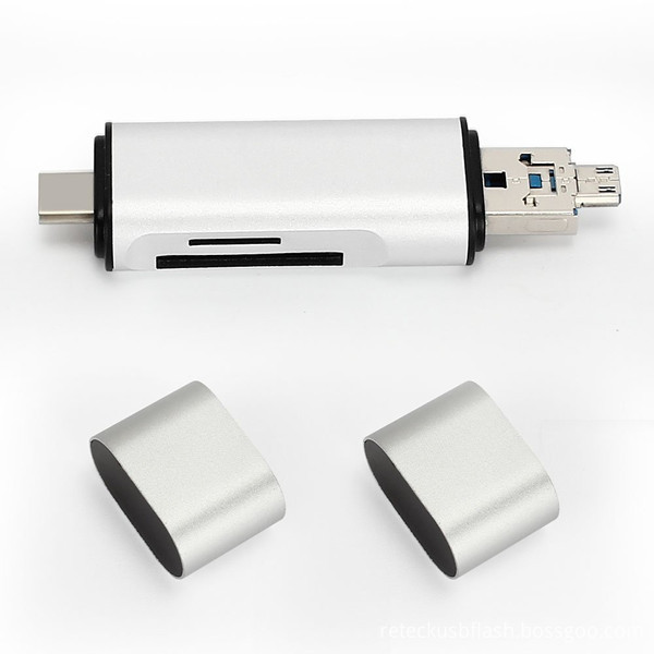
OTG Functions Usb Type C 3.1 Flash Drive
Unique 3 in 1 Multifunctional Design: USB 3.1 Type C, USB Type A and Micro USB card reader.
Support OTG, allows you to transfer and share your content between new-generation Smartphones, tablets and laptops with USB Type-C ports.
USB 3.1 Type C Compatible: Connect your TF card with the latest USB-C devices.
Fully compatible with USB 2.0, the reader transfers files quickly and efficiently. Even bulky files like HD video will transfer within minutes.

We are a professional Chinese manufacturer of Usb Flash Drive , and looking forward to your cooperation!
3 in 1 Dual Port USB Flash Drive, Type C USB Flash Drive, 2017 Usb C Type Flash Drive, 8GB USB Flash Drive For MacBook Type-c Mobile Phone
Reteck Electronic Co., Ltd. , https://www.reteck.com