Among many environmentally friendly light source applications, LED is a light source technology that is more energy efficient and easier to assemble than other light source solutions. Among the lighting source applications, high power white LEDs are the most frequent light emitting components, but Although white LEDs have been developed in terms of luminous efficiency and single power performance, in fact, white LEDs still have problems such as uniformity of illumination and lifetime of packaging materials, especially in the application of heat dissipation of chips, which is the first requirement for the development of LED light source applications. The problem of improvement.
High-power white LEDs are used in daily lighting applications. In fact, after environmental protection light sources have received increasing attention, they have become the primary choice for developing environmentally friendly light sources. However, there are still many technical bottlenecks in white LEDs that have yet to be overcome. At present, there are related improvement schemes to enhance the design bottleneck of white LEDs in terms of uniformity of illumination, life of packaging materials, heat dissipation enhancement, etc., and to carry out key functions and performance. Improvement.
Environmentally friendly light source demand increases high power white LED application outlet
The main reason why LED light source is favored is that it has long product life, high light-to-electric conversion efficiency, and material properties can be embedded in any plane. However, in the development of daily lighting sources, due to the need to achieve practical "lighting" requirements, the original LEDs for indication purposes can not directly correspond to lighting applications, must be strengthened from the chip, package, carrier board, production technology and external circuits. To achieve the high power, high brightness lighting effects required for lighting applications.
As for the market demand level, the white LED developed for the lighting application market can be said to be a product with higher usage in the future, but in order to achieve the utility, the white LED must be improved for the lighting application. One is to strengthen the LED chip , for example, to increase its light-to-electric conversion efficiency, or to increase the chip area, so that the luminous amount (light flux) of a single LED reaches its design limit. Secondly, it is a more compromised design. If the size of a single LED chip is continuously difficult, and the multi-chip LED chip is packaged in the same light source module, it is also a practical technical solution that can reach the above method. .
Meets low-cost, high-brightness design requirements in a multi-chip package
As for the inspection of industrial practice requirements, due to mass production flexibility, design difficulty and control of product yield/cost, LED chips continue to meet the design bottleneck of cost and yield. A glimpse of the design of the chip area may be difficult, not technical and production technology, but in terms of cost and efficiency considerations, large-area LED chips cost higher, and changes to actual manufacturing needs The design flexibility is low.
Instead, the integrated packaging method of multiple chips is used to equidistantly arrange a plurality of LED small chips on the carrier board, and the entire package of the optical package materials is connected by wire bonding to form a light source module product, and more The chip package can be integrated into a light source module equivalent to a large chip after secondary chip processing, but it is more flexible in terms of manufacturing flexibility than the single-chip LED light source component.
At the same time, the multi-chip LED chip module solution, the production cost can also be greatly reduced due to the cost of the chip, which is equivalent to the lower cost development option under the same luminous flux of the monolithic design.
Multi-chip integrated light source module still needs to consider cost maximization
Another development direction is to continuously increase the area of ​​the LED chip and obtain high brightness and high luminous flux output through a large area. However, the area of ​​the oversized LED chip may also be less than expected by the design. The common improvement scheme is to modify the structure of the polycrystal to improve the surface of the chip. However, the related improvement scheme also easily affects the heat dissipation efficiency of the chip itself, especially in the light source. Most of the applied LED modules are required to be driven at high power to obtain higher luminous flux, which will cause the high heat collected by the chip junctions during the illuminating process of the chip to be easily dissipated, affecting the application flexibility and main/passive of the module products. Thermal design.
In the general design scheme, according to the analysis, the chip size of 7mm2 is adopted, and the luminous efficiency is the best, but the 7mm2 large chip is difficult to control the yield and light performance, and the cost is relatively high; instead, the multi-chip chip is used, such as 4 A piece or 8 pieces of low-power chips are used for secondary processing on the carrier board to form an LED light source module with the package material, which is a design scheme for the LED light source module product capable of rapidly developing the required brightness and power performance.
For example, manufacturers of light source products such as Philips, OSRAM, and CREE have introduced LED light source module products that integrate 4, 8 or more small LED chip packages. However, such high-brightness component schemes using multiple LED chip architectures have also caused some design problems. For example, multiple LED chip package packages must be combined with built-in insulation materials to avoid short-circuiting of individual LED chips; such a process is relatively There are many more programs in a single-chip design, so even if you can save costs compared to a single-chip solution, the cost gap between the two solutions can be reduced by the extra insulation process.
Application chip surface process improvement can also enhance LED light output
In addition to increasing the chip area or number is the most straightforward method, there is another improvement in luminous efficacy for the material properties of the chip itself. For example, an uneven surface structure can be fabricated on the LED sapphire substrate, and the irregular light-designed surface is used to enhance the LED light output, that is, a texture surface crystal structure is established on the surface of the chip.
OSRAM uses this solution to develop ThinGaN high-brightness products. The metal film material is first formed in the InGaN layer, and then the stripping process is performed, so that the surface after peeling can indirectly obtain higher light output! OSRAM claims that this technology allows the same chip to achieve 75% light extraction efficiency.
On the other hand, the development thinking of OMRON in Japan is quite different. The same is the light extraction efficiency of the chip. OMRON attempts to use the planar light source technology to reflect, guide and control the chip light source with LENS optical system. The light loss problem common to LED products of type package structure further improves the design structure, and uses the double-layer reflection effect to control and enhance the light extraction amount of the LED. However, this packaging technology is relatively more complicated and costly, so most of them are only used. Designed for LCDTV backlight modules.
ZGAR PCC KIT
ZGAR PCC KIT
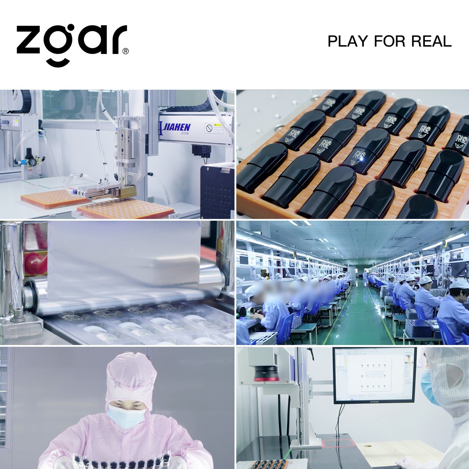
ZGAR electronic cigarette uses high-tech R&D, food grade disposable pod device and high-quality raw material. All package designs are Original IP. Our designer team is from Hong Kong. We have very high requirements for product quality, flavors taste and packaging design. The E-liquid is imported, materials are food grade, and assembly plant is medical-grade dust-free workshops.
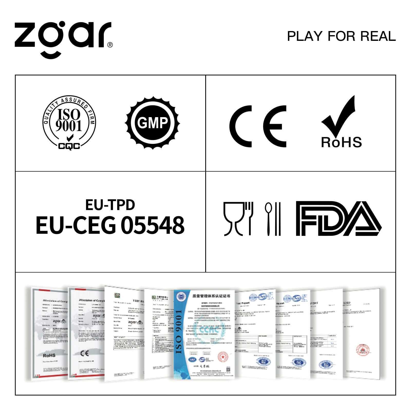
From production to packaging, the whole system of tracking, efficient and orderly process, achieving daily efficient output. We pay attention to the details of each process control. The first class dust-free production workshop has passed the GMP food and drug production standard certification, ensuring quality and safety. We choose the products with a traceability system, which can not only effectively track and trace all kinds of data, but also ensure good product quality.
We offer best price, high quality Vape Device, E-Cigarette Vape Pen, Disposable Device Vape,Vape Pen Atomizer, Electronic cigarette to all over the world.
Much Better Vaping Experience!


ZGAR PCC KIT E-Cigarette Vape Pen,ZGAR PCC KIT Disposable Device Vape,PCC SET,ZGAR PCC KIT Vape Pen Atomizer,ZGAR PCC KIT Disposable E-Cigarette OEM vape pen,ZGAR PCC KIT electronic cigarette
Zgar International (M) SDN BHD , https://www.zgarvapepen.com

