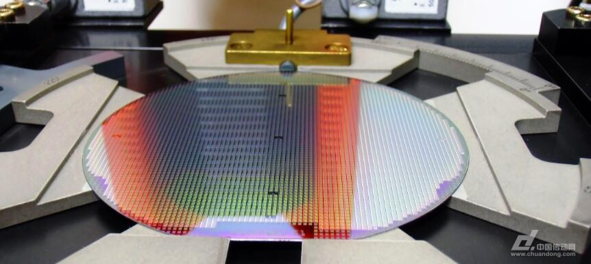
[The mass production of EUV technology has entered the final stage of sprint, and the ultra-violet stepper will soon be available] With engineers competing to solve intricate and related issues, 20 years of new generation of lithography tools have finally come to the last Stage--Although the mass production of EUV stepper faces complex problems and pressing time, experts are still optimistic.
The good news is that the semiconductor industry is consolidating and actively promoting technological advances; for example, AnSteegen, executive vice president of technology and systems at Belgian research firm Imec, said: “In the past, there may be one company that pioneered the latest semiconductor technology, but now it is almost All logic technology suppliers are jumping in, clenching their teeth and taking risks."

Imec is a long-term partner of ASML, the Dutch EUV lithography equipment manufacturer. Together with foundries and semiconductor suppliers, Imec is now aiming to solve the problem of the size of a room that will be used to make a new generation of chips. The last few major problems with the equipment; Steegen pointed out in an interview with EETimes at the Imec annual technology forum that this is very much like the FinFET transistor that was introduced in 2008, and it is a very important but challenging key to semiconductor performance improvement.
She said: “People compare the worst situation of the next generation node and the best situation of the old node. Now all parties agree that FinFET is a component with ultra-high performance; the lesson I’ve learned is to be skeptical about everything. ... There is room for improvement in future semiconductor process technologies so that SoC designers can get what they want."
When I was chatting with an EUV development veteran with 32 years of work experience waiting in line at the headquarters of Imec, he simply said: “There is a lot of pressure...but we are making progress.â€
Indeed, Samsung’s foundry rushed to introduce EUV at the end of this year at the 7-nm process. The company’s goal is to surpass its largest competitor, TSMC, which is using existing immersion lithography equipment. In the case of the 7-nanometer design film, Taiwan Semiconductor Manufacturing Co., Ltd. and another foundry giant, GlobalFoundries, will not fall. They plan to use EUV to mass-produce the enhanced 7-nm process next year.
Imec expects DRAM makers to adopt EUV technology at the D14+ node--which should be half-pitched to 20 nanometers by 2021.
Currently Imec has two technical development priorities that help to alleviate the issue of line-edgerness and eliminate so-called stochastics, random errors, etc. resulting in contact misses (createmissing), contacts Interruptions (kissingcontacts). Those errors were first discovered this year at the critical 15nm critical dimension for next-generation 5-nanometer nodes, but the researchers said they also see the same problem at 7nm.
Steegen expects that there will be a hybrid solution that will use a combination of scanner settings, photoresist materials, and post-processing methods to continue the broken lines, smooth out the roughness, or fill missing touches. point.
Wafers can provide higher doses of EUV light sources - such as 80millijoules/cm2 - to expand the process window, but this will slow down the production process; Steegen said: "The first implementation The highest dose decision right lies with each foundry."

Engineers are using a series of mask adjustments, stepper settings, photoresist selection, and post-processing methods to solve the problem of random errors in EUV (Source: Imec)
Hybrid solutions and relaxed design rules
Imec is developing a way to predict and locate where random errors may occur in the design to provide a view of the process tolerance range; but finding defects is often very dependent on fast e-beam inspection systems.
As process nodes come to single-nanometer sizes, researchers have begun to attribute defects to small details; for example, the number of photons in an EUV exposure will affect chemically amplified resisters, while other types of light Resist performance can also vary due to the orientation of the embedded metal molecules.
For this Steegen said: "Not all photoresists are equally effective. Their role in different substrates will also be unique... We are still going through some basic learning."
In order to simplify the transition of process generation, GlobalFoundries adopted a phased EUV strategy, using only five layers of metal at the relatively loose 7-nanometer node; the company’s chief technology officer Gary Patton said in an interview at the Imec Technology Forum: “We can use lower doses. Operate and achieve good production."
Patton revealed that GlobalFoundries will use infiltrating lithography later this year for the first 7nm design. It is an AMD processor; followed by an IBM processor and then several ASICs.
GlobalFoundries made the 7nm node pitch and SRAM cell similar to that of TSMC, allowing chip designers such as AMD to use two foundries simultaneously; he said that AMD's demand will be higher than we have, so We have no opinion on this matter (AMD also commissioned TSMC production)."
However, GlobalFoundries skips the 5-nanometer node while developing a 10-nanometer node, and the company believes that the former will have modest incremental gains; while the company is seeking financial and technical partners for the next-generation process, it is likely to move toward 3nm. Node is moving forward.

The lithography technicians now view the yield issue as a top priority for EUVs (Source: Imec)
Maintain optimism while facing numerous challenges
Despite numerous challenges, Patton remained optimistic; he believes that despite the slowdown in the growth of the smart phone market, the industry has evolved into the era of AI, "a new fabless IC company has surged." At the same time, GlobalFoundries' FD-SOI process will have 75 design partners by the end of the year and 36 designs have been obtained.
"A lot of people were watching the FD-SOI on the sidelines last year. Whether or not FD-SOI can be achieved is clear." Patton pointed out that the process technology can support designs as low as 0.4V, and will produce Grade 2 vehicle regulation versions this fall.
GlobalFoundries and Imec's senior executives are still optimistic about the progress of the overall semiconductor technology roadmap. However, some engineers have begun to talk openly about the fact that the increase in transistor speed has generally come to an end. The progress in transistor density and performance is a decrease in one node compared to a node.
Imec is assisting wafer foundries to develop a series of performance-boosting technologies to reinforce this, including simplified cell tracks, buried power rails, and on-die circuit stacks.
"Generally speaking, I don't see diminishing returns," Steegen said. "I'm optimistic about the development of 3nm and 2nm logic process nodes and memory technology. We have enough resources... So the design engineer will see the chip area. Shrinking, but they may need to make some changes in the design."
As a result, Imec's chip miniaturization core project continues to grow at a rate of 5 to 10% a year. CEO of Imec Luc Vanden Hove said: “Ten years ago, we expected our work on advanced CMOS process technology to continue to grow. Because of industry consolidation, the opposite is true.†He pointed out that Imec's related projects have increased due to new topics such as AI accelerator chips and DNA storage.
Description of self closing braided sleeving
PET White Self Wrapping Split Braided Sleeving for cable management (PET woven mesh tube) is braided by environment friendly polyester monofil. PET is with good flexibility, fire resistance, abrasive resistance and thermal insulation performance. The sleeving are smooth surface, bright color, various patterns.
self-closing wrap offers innovative solutions for the protection of breakout areas and provides easy removal when is necessary an inspection or maintenance of cables. The special open structure allows to be installed after other components, for example copper terminals and connectors.
Features of Self Closing Braided Wrap For Cable Management
• Easy, cost and labor effective installation
• More flexible than split convoluted or spiral wrap
• 50% edge overlap
• Cut and abrasion resistant
• Halogen free
• Retains shape and rigidity throughout -50°C to 150°C temperature range
• melt temp. 250°C
Split Braided Sleeving,Split Loom Cable Wrap ,Self Cable Sleeving,Pp Self Wrap Sleeve
Shenzhen Huiyunhai Tech.Co.,Ltd , https://www.hyhbraidedsleeve.com