PCB layout engineers work on thousands of traces every day on the board, and various packages are used to repeat the work of pulling cables. Many people may feel that they are very boring tasks. Looks like a software operation porter, in fact, the designer must choose between various design rules in the process, taking into account all aspects of performance, cost, process, etc., but also pay attention to the rational layout of the board layout, and did not look so Simple, need more wisdom. Good work habits will benefit you, make your design more reasonable, make production easier and perform better. Here are six good habits for you to benefit from.
(a) Details determine success or failure
PCB design is a meticulous task that requires carefulness and patience. The mistakes often made by newcomers who just start designing are some details. The device pins are wrong, the device package is wrong, the pin sequence is reversed, and so on. Some of them can be solved by flying wires, and some may make a board directly become a waste product. When checking the package, check it again. Before the board is printed out, compare the package with the actual device. Take a look, check it again is not obsessive-compulsive disorder, just make these low-level mistakes easy to avoid. Otherwise, the beautifully designed board, covered with flying lines, is far from excellent.
(b) Learn to set rules
The implementation of the advanced PCB design software requires not only the layout rules but also some simple and easy-to-use PCB tools. After all, the human brain is not a machine, it will inevitably have negligence and mistakes. So set up some easy-to-neglect problems in the rules, let the computer help us check, try to avoid making some low-level mistakes. In addition, a perfect set of rules can better regulate the work behind. The so-called grinding knife does not mistakenly cut the firewood. The more complex the scale of the board is, the more important it is to set the rules. Nowadays, many EDA tools have auto-wiring capabilities. If the rules are set in enough detail, let the tool help you design for yourself. Isn't it more pleasant to have a cup of coffee on the side?
(3) The more you consider for others, the less your own work
When doing PCB design, consider as many end-users as possible. For example, if you are designing a development board, you should consider placing more silkscreen information when designing the PCB. This will make it more convenient to use. It is not used to search for schematics or to find support from designers. If you are designing a mass-produced product, you need to consider more of the problems that will be encountered in the production line, the same type of device as far as possible in the same direction, the device spacing is appropriate, the board edge width and so on. The earlier these issues are considered, the less impact it will have on the design behind it, and the fewer workloads that will be supported later and the number of board changes. It seems that the time spent on design starts to increase, actually reducing the amount of follow-up work. In the case that the board space signal allows, try to place more test points and improve the testability of the board. This will also save more time in the subsequent debugging stage and provide more ideas for finding problems.

(d) Drawing the schematic
Many engineers feel that the layout work is more important, and the schematic is to generate a netlist to facilitate inspection of the PCB. In fact, the role of the schematic in the subsequent circuit debugging process will be greater. Whether it is to find problems or communicate with colleagues, or the schematic is more intuitive and more convenient. In addition, develop the habit of labeling in the schematic diagram, the problem that each part of the circuit should pay attention to in the layout is marked on the schematic diagram, it is a good reminder to oneself or to others. The hierarchical schematic diagram divides the circuits of different functional modules into different pages, so that whether the drawings are read or reused later can significantly reduce the workload. Using a mature design is always less risky than designing a new circuit. Every time I see all the circuits on a drawing, a dense device, the head can be a big circle.
(E) Conduct circuit layout well
The eager engineers finished drawing the schematics. After importing the netlist into the PCB, they couldn't wait to put the device away and start pulling. In fact, a good PCB layout will make it easier for you to work on the rear cable and make your PCB work better. Each board will have a signal path, and the PCB layout should follow this signal path as much as possible so that the signal can be smoothly transmitted on the board. People do not like to walk the maze and the signal is the same. If the schematic is designed according to the module, the same is true for the PCB. According to different functional modules, the board can be divided into several areas. Separate analog signals, separate power signals, separate heat-generating and susceptibility devices, large-sized devices not too close to the edge of the board, attention to RF signal shielding, etc.... Take a minute to optimize the layout of the PCB. Save more time when pulling the cable.
(6) Trying to do Simulation
Simulation is often something PCB design engineers do not want to touch. Some people may say that even if I simulate, the actual PCB and simulation results will still be different, then I'm also wasting time doing simulations? I do not simulate the board is not the same work? The idea is very helpless. Designing once or twice is not a problem. It does not mean that there will be no problem in the future. Although there are differences between the simulation results and the actual results, the simulation can show the correct trend of change. According to the trend, we can make our own judgments. It may be difficult at first, and it is normal for simulation parameters to confuse the simulation model. As long as you start, slowly, and slowly accumulate, you will realize the importance of simulation. Before the completion of the board to determine the location of the problem that is prone to problems, to solve it in advance to avoid problems. If you do more simulations, you will fundamentally understand the causes of the problems and will greatly help you improve your design capabilities.
Everyone in the actual work, if you can take note of the above mentioned issues, develop a good work habit in the work, I believe that with the gradual improvement of personal ability, will complete more and better designs.
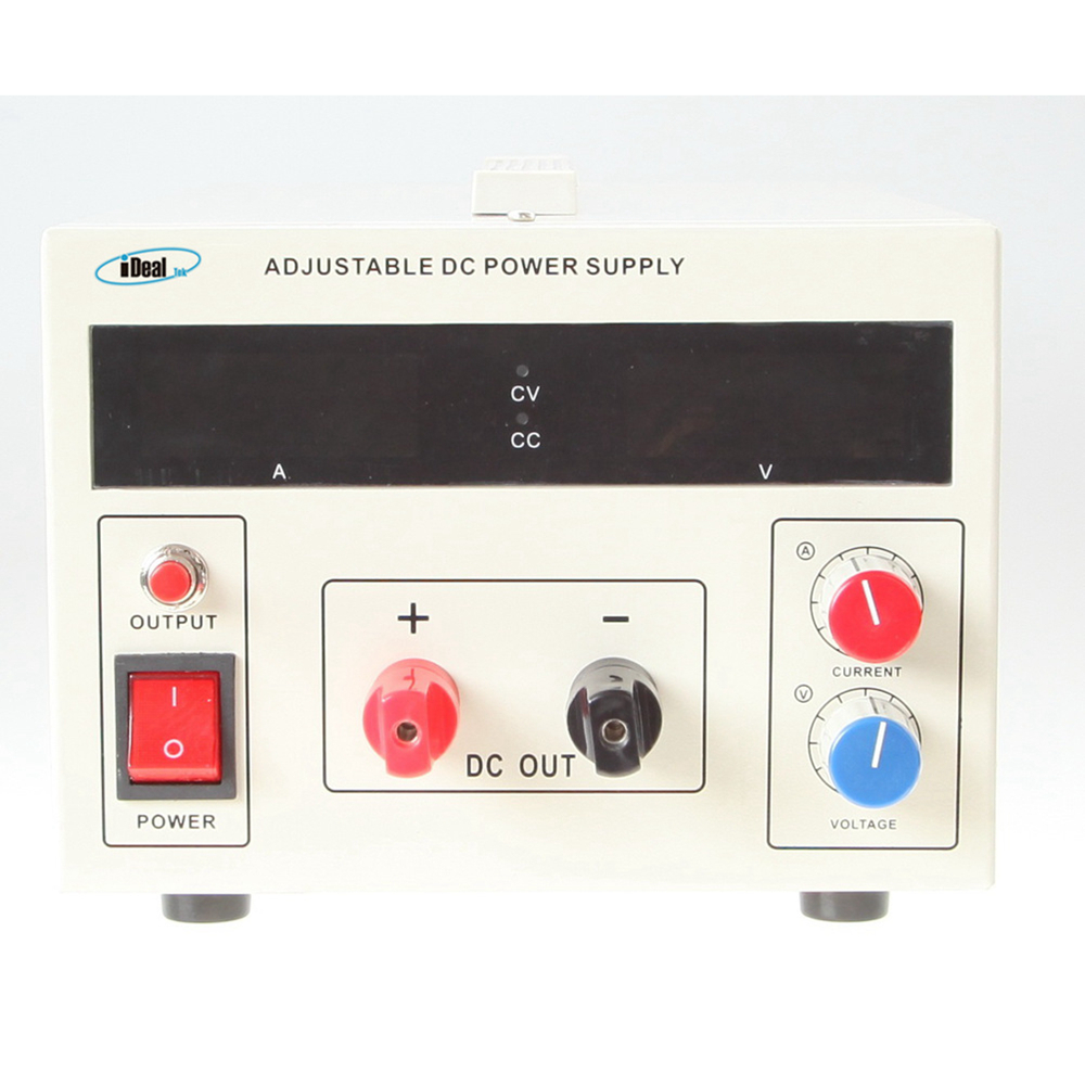
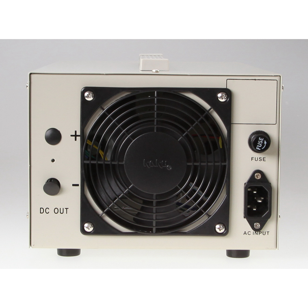
SMP series Bench DC Power Supplies are economical, MOSFETs-based, high switching speed, high power density desktop DC power supplies with output power covering 300W ~ 6KW, and maximum voltage up to 800VDC.
Compared with IGBT-based DC switching power supplies, MOSFET-based switching power supplies have a higher switching frequency, making this series Benchtop DC power supplies can use smaller semiconductor devices and LC filter units while ensuring low ripple, high precision, and fast response characteristics of the Benchtop Laboratory Power Supplies DC output. Which gives more space to use a smaller chassis size at the same output power, resulting the high-power density feature of this series Benchtop AC DC power supplies.


The main design purpose of this series of Bench AC-DC power supplies is to fulfill the needs of small laboratory test, precise experiment and universities.
At present, this series of Bench AC DC power supplies below 1KW adopts desktop chassis to match laboratory applications, they are mainly used in LED testing, small electroplating, heating of new materials, electrical component testing and other applications.
Bench DC Power Supplies, Desktop DC Power Supplies, Bench Laboratory Power Supplies, Benchtop AC DC Power Supplies, Bench AC-DC Supplies
Yangzhou IdealTek Electronics Co., Ltd. , https://www.idealtekpower.com