When the computer is working, it is performed under the unified clock pulse control. This pulse is issued by the timing circuit in the microcontroller controller. The timing of the MCU is the time sequence of the control signals required by the CPU when executing the instructions. In order to ensure the synchronous operation between the components, the internal circuit of the MCU should strictly control the timing under the unique clock signal, before learning the timing of the 51 MCU. Let's first understand some of the concepts related to timing.
Since the computer is operating under a unified clock pulse, how does its clock pulse come from?
To provide timing for our computer CPUs, we need the relevant hardware circuits, the oscillator and the clock circuit. The 8051 microcontroller we have studied has a high-gain inverting amplifier. The function of this inverting amplifier is to form the oscillator. However, to form the clock, some additional circuits need to be added externally. The clock generation of the 8051 microcontroller has the following two methods:
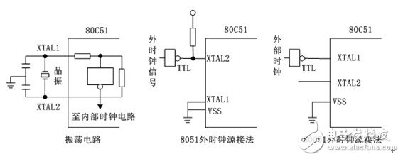
First, the internal clock mode:Using the internal oscillator of the microcontroller, and then connecting the crystal oscillators at the XTAL1 (18-pin) and XTAL2 (19-pin) pins, a stable self-excited oscillator is formed, and the pulse is directly sent to the internal clock circuit, and the external crystal oscillator is connected. When the capacitance of the crystal oscillator is generally selected to be about 30 PF; these two capacitors have a fine-tuning effect on the frequency, and the frequency range of the crystal oscillator can be selected between 1.2 MHz and 12 MHz. In order to reduce the parasitic capacitance and better ensure that the oscillator works stably and reliably, the oscillator and capacitor should be installed as close as possible to the microcontroller chip. (Hint, the learning kits provided by this site all use this clock method).
Second, the external clock mode:This method uses an external oscillation pulse to access XTAL1 or XTAL2. HMOS and CHMOS MCU external clock signal access mode is different, HMOS type MCU (such as 8051) external clock signal is injected into the internal clock circuit directly from the XTAL2 pin, the input terminal XTAL1 should be grounded. Since the logic level of the XTAL2 terminal is not TTL, it is recommended to connect an external resistor. For CHMOS type MCU (such as 80C51), since the signal of the internal clock generator is taken from the input of the inverter, when an external clock source is used, the external clock signal is connected to XTAL1 and XTAL2 is left floating. As shown below

The external clock signal becomes an internal clock signal through a two-way flip-flop. The duration of the high and low levels is required to be greater than 20 ns, which is generally a square wave with a frequency lower than 12 MHz. The on-chip clock generator is the above-mentioned two-way flip-flop, which provides a 2-shot clock signal to the chip.
As mentioned above, when the computer is working, it is performed under the unified clock pulse control. Since the number of bytes of the instruction is different, the time required to take these instructions is different. Even if the instructions have the same number of bytes, the execution time of the different instructions is not necessarily the same, that is, the required instructions are not necessarily the same. The number of beats is different. In order to facilitate the analysis of the CPU timing, generally several cycles are specified according to the execution process of the instruction, that is, the clock cycle, the machine cycle and the instruction cycle, which are also called timing timing units, which are respectively explained below.
Clock cycle
The clock cycle is also called the oscillation cycle and is defined as the reciprocal of the clock pulse. It can be understood that the clock cycle is the reciprocal of the external crystal of the MCU, such as the 12M crystal oscillator, which has a time period of 1/12 us. It is the most basic computer. The smallest unit of time.
In one clock cycle, the CPU only performs one of the most basic actions. For a single-chip microcomputer, if a clock frequency of 1 MHz is used, the clock period is 1 us; if a clock frequency of 4 MHz is used, the clock period is 250 us. Since the clock pulse is the basic working pulse of the computer, it controls the working rhythm of the computer (so that every step of the computer is unified to its pace). Obviously, for computers of the same model, the higher the clock frequency, the faster the computer will work. However, since different computer hardware circuits and devices are not identical, the required clock frequency range is not necessarily the same. The clock range of the 8051 microcontroller we studied is 1.2MHz-12MHz.
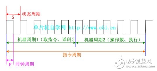
In the 8051 microcontroller, one clock cycle is defined as one beat (indicated by P), and two beats are defined as one state cycle (indicated by S). Please refer to the timing diagram below.
Machine cycle
In the computer, in order to facilitate management, the execution process of an instruction is often divided into several stages, and each stage completes a work. For example, fetch instructions, memory reads, memory writes, etc., each of which is called a basic operation. The time required to complete a basic operation is called the machine cycle. In general, a machine cycle consists of several S cycles (state cycles). One machine cycle of the 8051 series MCU is composed of six S cycles (state cycles). As mentioned above, one clock cycle is defined as one beat (indicated by P), and two beats are defined as one state cycle (indicated by S). The machine cycle of the 8051 microcontroller consists of six state cycles, that is, one machine cycle = 6 state cycles = 12 clock cycles. See the timing diagram below.
Instruction cycle
The instruction cycle is the time required to execute an instruction and is typically composed of several machine cycles. The number of machine cycles required varies depending on the command. For some simple single-byte instructions, in the instruction fetch cycle, after the instruction is fetched into the instruction register, the instruction is decoded and executed, and no other machine cycles are needed. For some more complex instructions, such as branch instructions, multiplication instructions, two or more machine cycles are required.
The relationship between the clock cycle, machine cycle, and instruction cycle is as follows.

An instruction that typically contains one machine cycle is called a one-cycle instruction, and an instruction that contains two machine cycles is called a two-cycle instruction.
In the MCS-51 instruction system, they can be divided into single-byte instructions, double-byte instructions, and three-byte instructions according to their length. The time required to execute these instructions is different, that is, the machine cycles they require are different, in the following forms:
· Single byte instruction single machine cycle
· Single byte instruction dual machine cycle
·Double byte instruction single machine cycle
Double-byte instruction dual machine cycle
· Three-byte instruction dual machine cycle
Single-byte instructions four machine cycles (such as single-byte multiply and divide instructions)
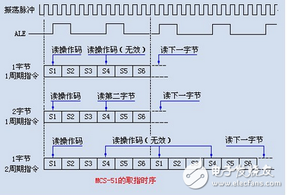
The following figure shows the instruction timing diagram of the MCS-51 series MCU:

The above figure shows the single-cycle and double-cycle fetch and execution timing. The ALE pulse in the figure is the strobe signal for latching the address. Obviously, the read-mapping operation is performed every time the MCU appears. As can be seen from the timing diagram, the signal is obtained after dividing the clock frequency by 6. In one machine cycle, the ALE signal is valid twice, the first time during S1P2 and S2P1, and the second time during S4P2 and S5P1.
Next, we will explain a few typical instruction timings.
· Single-byte single-cycle instructions:
A single-byte single-cycle instruction performs only one read instruction operation. When the second ALE signal is valid, the PC does not increment by one, and then the original instruction is read, which is an invalid read operation.
Double-byte single-cycle instructions:
The ALE signal of this type of instruction is valid only when the first ALE signal is valid and the operation code is read. When the second ALE signal is valid, the operand is read.
· Single-byte dual-cycle instructions:
Four machine instruction operations are required for two machine cycles, but only one read operation is valid, and the last three read operations are invalid.
A single-byte, two-cycle instruction has a special case. For instructions such as MOVX, when executing such an instruction, the instruction is first read in the ROM, and then the external data memory is read or written, first in the first machine cycle. The opcode of the secondary read instruction is valid, while the second read instruction is invalid. In the second instruction cycle, the external data memory is accessed. At this time, the ALE signal has no effect on its operation, that is, there is no more read instruction operation.
In the timing diagram on the previous page, we only describe the read status of the instruction, but do not draw the instruction execution timing, because each instruction contains a specific operand, and there are many types of operands, which are not listed here. Interested readers can refer to related books.
· External program memory (ROM) read timing

The 8051 external program memory read timing diagram on the right, as can be seen from the figure, the P0 port provides the lower 8-bit address, and the P2 port provides the upper 8-bit address. Before the end of S2, the lower 8-bit address on the P0 port is valid, and then appears. On the P0 port, it is no longer the lower 8-bit address signal, but the command data signal. Of course, there is a buffering excessive time between the address signal and the command data signal. This requires that the lower 8 bits must be placed in S2. The address signal is latched. At this time, the ALE strobe pulse is used to control the latch to latch the lower 8-bit address, while the P2 port only outputs the address signal, and without the command data signal, the entire machine cycle address signal is valid. Therefore, there is no need to latch this address signal.
To read an instruction from the external program memory, there must be two signals to control. In addition to the above ALE signal, there is also a PSEN (external ROM read strobe). As you can see from the above figure, PSEN is valid from S3P1 until The address signal is sent out and the data of the external program memory is read into the CPU before it expires. The second read instruction operation is executed from S4P2.
External data memory (RAM) read timing
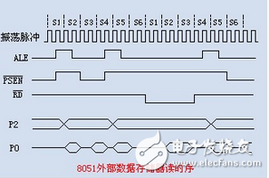
The 8051 external data memory read and write timing diagram on the right, the instruction to be executed read from the ROM, and the CPU access to the external data storage is the read or write operation of the RAM, which belongs to the execution cycle of the instruction, which is worth mentioning. The read or write is two different machine cycles, but their timing is similar. We only analyze the read timing of the RAM.
The last machine cycle is the fetching phase, in which the instruction data is read from the ROM, and the next cycle begins to read the contents of the external data memory RAM.
After the end of S4, the address in the RAM to be read is first placed on the bus, including the lower 8-bit address A0-A7 on the P0 port and the upper 8-bit address A8-A15 on the P2 port. When the RD strobe pulse is active, the RAM data is read into the CPU through the P0 data bus. The ALE signal of the second machine cycle still appears, and an external ROM read operation is performed, but this time the read operation is an invalid operation.
When writing to the external RAM, the CPU outputs WR (write strobe signal) and writes the data to the external memory through the P0 data bus.
The main pain points in obtaining customers in foreign trade are fierce market competition, high customer acquisition costs, low customer stickiness, and single marketing methods. With the changes in the market environment, traditional marketing methods have been unable to meet customer needs. Enterprises need innovative marketing methods and technical means to improve customer stickiness and loyalty, reduce customer acquisition costs, in order to obtain more business opportunities in the fierce market competition.
koko
2222Bossgoo(China)Tecgnology.
(Bossgoo(China)Tecgnology) , https://www.cn-gangdao.com