To the conductive characteristics, when it is used in the circuit, the first reaction is rectification, and there are not many other characteristics and applications of the diode. It is also recognized that the unidirectional conduction characteristics of the diode can be grasped, and various diodes can be analyzed. Circuits, in fact, such ideas are wrong, and to some extent harm themselves, because this directional thinking affects the analysis of the working principle of various diode circuits, many diode circuits can not be explained by unidirectional conductive characteristics Its working principle.
In addition to the unidirectional conduction characteristics of diodes, there are many characteristics. In many circuits, the unidirectional conduction characteristics are not used to analyze the working principle of the circuit formed by the diodes. It is necessary to grasp more characteristics of the diodes in order to correctly analyze these circuits, for example, A simple DC voltage regulator circuit composed of a diode, a temperature compensation circuit composed of a diode, and the like.
1 diode simple DC voltage regulator circuit and fault handling
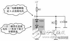
The diode simple voltage regulator circuit is mainly used in some local DC voltage supply circuits. Because of its simple circuit and low cost, it is widely used. In the simple voltage regulator circuit of the diode, the tube voltage drop of the diode is mainly used. The tube voltage drop characteristic of the diode: the tube voltage drop is basically unchanged after the diode is turned on. For a silicon diode, the tube voltage drop is about 0.6V, and for a germanium diode, it is about 0.2V. As shown in Figure 1.1, it is a simple DC voltage regulator circuit composed of three ordinary diodes. VD1, VD2 and VD3 in the circuit are common diodes, which are connected in series to form a simple DC voltage regulator circuit.

Figure 1.1 Simple DC voltage regulator circuit composed of 3 ordinary diodes
1.1 circuit analysis ideas
It is difficult to analyze the working principle of a circuit that has never been seen before, and it is more difficult for beginners whose basic knowledge is not comprehensive. The analysis of this circuit is mainly explained as follows.
(1) It can be seen from the circuit that three diodes are connected in series. According to the characteristics of the series circuit, the three diodes will be turned on at the same time if they are turned on, and will be cut off at the same time.
(2) According to the judgment principle of whether the diode is turned on, the positive electrode of the diode is connected with a voltage much higher than the negative electrode, whether it is DC or AC voltage, and the diode is in an on state at this time. It can be seen from the circuit that the positive electrode of VD1 is connected to the DC working voltage +V in the circuit through the resistor R1, and the negative electrode of VD3 is grounded, so that a sufficient forward DC voltage is applied to the three series diodes. From this analysis, it can be seen that the three diodes VD1, VD2 and VD3 are turned on under the action of the DC operating voltage +V.
(3) It can also be seen from the circuit that the AC signal voltage is not added to the three diodes because a large-capacitance capacitor C1 is connected between the point A of the VD1 positive terminal and the ground, and any AC voltage at point A is bypassed. To the ground.
1.2 Diode can stabilize DC voltage principle
In the circuit, three diodes are turned on under the forward bias of the DC operating voltage. The function of this circuit after conduction is to stabilize the DC voltage at point A in the circuit. It is well known that the inside of the diode is a PN junction structure. The PN junction has many characteristics in addition to the unidirectional conduction characteristics. One of them is that the tube voltage drop is substantially constant after the diode is turned on, and is turned on for the commonly used silicon diode. The voltage drop between the positive and negative electrodes was 0.6V.
According to this characteristic of the diode, it is convenient to analyze the working principle of a simple DC voltage regulator circuit composed of a common diode. After the three diodes are turned on, the tube voltage drop of each diode is 0.6V, then the DC voltage drop after three series connections is 0.6 × 3 = 1.8V.
1.3 Fault detection method
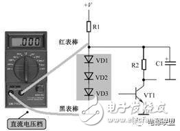
The most effective way to detect the three diodes in this circuit is to measure the DC voltage on the diode, as shown in Figure 1.2. If the measured DC voltage is about 1.8V, it means that 3 diodes work normally; if the measured DC voltage is 0V, it is necessary to measure whether the DC working voltage +V is normal and whether the resistor R1 is open, regardless of the 3 diodes, because 3 diodes At the same time, the possibility of breakdown is small; if the measured DC voltage is greater than 1.8V, check one of the three diodes for an open fault.

Figure 1.2 Schematic diagram of DC voltage wiring on the measuring diode
1.4 Circuit Failure Analysis
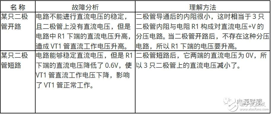
As shown in Table 1.1, this diode circuit failure analysis
Table 1.1 diode circuit failure analysis

1.5 circuit analysis details
The details of the analysis of the above simple DC voltage regulator circuit are described below.
(1) In the circuit analysis, the unidirectional conductivity of the diode can be used to know that the diode is in the on state, but it does not explain the specific effects of the diodes on the circuit after being turned on, so only the unidirectional conduction characteristics are used. Can correctly analyze the working principle of the circuit.
(2) Among the many characteristics of the diode, only the voltage drop after the conduction is substantially constant can explain the function of the circuit most reasonably. Therefore, according to this point, it can be determined that the circuit is used to stabilize the DC at point A in the circuit. Operating Voltage.
(3) When there are many components in the circuit, we must try to figure out the main components that realize the circuit function, and then carry out analysis around it. The main characteristics of the component are used in the analysis to make a reasonable explanation.
2 diode temperature compensation circuit and fault handling
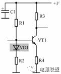
It is well known that there is a voltage drop of about 0.6V (referred to as the PN junction of silicon material) after the PN junction is turned on, and the PN junction also has a temperature-related characteristic: the voltage drop after the PN junction is turned on is substantially the same, but not The pressure drop across the PN junction decreases slightly with increasing temperature. The higher the temperature, the more the amount of voltage drop. Of course, the absolute value of the voltage drop across the PN junction is quite small for 0.6V. The characteristics can constitute a temperature compensation circuit. As shown in Figure 2.1, a temperature compensation circuit is constructed using diode temperature characteristics.

Figure 2.1 Diode Temperature Compensation Circuit
For beginners, it is an amplifier that does not understand the components such as VT1 in the circuit, which is not good for analyzing the working principle of this circuit. In the circuit analysis, familiar with the unit circuit function composed of components such as VT1 has a positive significance for analyzing the working principle of VD1. Understand the function of the unit circuit, all circuit analysis can be carried out around it, so that it is targeted and more effective.
2.1 Need to understand the deep circuit working principle analysis This circuit working principle needs to understand the following two deep circuit principles.
(1) VT1 constitutes an amplifier circuit, which requires good stability for the amplifier. One of them is that the quiescent current of the triode cannot be changed when the temperature changes, that is, the VT1 base current cannot change with temperature. Otherwise, the work stability is not good. Understanding this temperature characteristic of the amplifier is very important to understand how the temperature compensation circuit formed by VD1 works.
(2) Transistor VT1 has a temperature-related bad characteristic. When the temperature rises, the base current of the triode VT1 will increase. The higher the temperature, the larger the base current, and vice versa. It is obvious that the temperature stability of the triode VT1 is not it is good. It can be seen that the temperature stability of the amplifier is poor due to the temperature characteristics of the triode.
2.2 Transistor Bias Circuit Analysis
In the circuit, the triode VT1 is given a certain DC bias voltage when it is in the amplification state, which is done by the bias circuit. R1, VD1 and R2 in the circuit form a voltage-dividing bias circuit, which provides a DC operating voltage for the base of the transistor VT1. The magnitude of the base voltage determines the magnitude of the VT1 base current. If the influence of temperature is not considered, and the DC operating voltage +V does not change, the VT1 base DC voltage is stable.
The base DC current of the transistor VT1 is constant, and the transistor can work stably.
In the analysis of the working principle of the diode VD1, it is necessary to clarify one point: VT1 is an NPN type triode, and its base DC voltage is high, then the base current is large; otherwise, it is small.
2.3 Diode VD1 temperature compensation circuit analysis
According to the position of the diode VD1 in the circuit, the analysis of its working principle mainly explains the following points:
(1) The positive pole of VD1 is connected to the DC working voltage +V through R1, and its negative pole is connected to the ground through R2, so that VD1 is in the conducting state under the action of DC working voltage +V. The key to understanding the conduction of the diode is that the voltage on the positive pole is higher than the voltage on the negative pole.
(2) It is not feasible to explain the role of VD1 in the circuit by using a 0.6V tube voltage drop after the diode is turned on, because the DC working voltage required by the VT1 base can be achieved by adjusting the resistance values ​​of R1 and R2. It is not necessary to adjust the VT1 base voltage by stringing diode VD1.
(3) The tube voltage drop temperature characteristic of the diode can correctly explain the role of VD1 in the circuit. Assuming the temperature rises, it is known from the characteristics of the triode that the base current of VT1 will increase. When the temperature rises, the tube voltage drop of the diode VD1 will decrease somewhat, and the voltage drop of the VD1 tube will cause the VT1 base voltage to drop somewhat, resulting in a decrease in the VT1 base current. It can be seen from the above analysis that after the addition of the diode VD1, the original temperature rises to increase the VT1 base current, and now the VD1 circuit can reduce the VT1 base current by a certain amount, thus stabilizing the base current of the triode VT1, so VD1 can function as a temperature compensation.
(4) The temperature stability of the triode is also poor in the process of temperature drop. When the temperature is lowered, the base current of the triode VT1 is reduced, which is also a poor performance of temperature stability. When the diode VD1 is connected, when the temperature drops, its tube voltage rises slightly, which causes the VT1 base DC operating voltage to rise. As a result, the VT1 base current increases, which also compensates for the instability of the triode VT1 temperature drop. .
2.4 Circuit Analysis Details
The details of the circuit analysis are described below.
(1) In circuit analysis, if a certain characteristic of a component can be used to reasonably explain its role in the circuit, it is likely that the circuit analysis is correct. For example, in the above circuit analysis, only the temperature characteristics of the diode can be used to reasonably explain the role of VD1 in the circuit.
(2) The temperature compensation of the temperature compensation circuit is bidirectional, that is, it can compensate for the instability of the circuit operation caused by the temperature increase or decrease.
(3) When analyzing the working principle of the temperature compensation circuit, it is necessary to assume the temperature rise or decrease, and then analyze the reaction process in the circuit to obtain the correct circuit feedback result. In the actual circuit analysis, it is possible to set the temperature compensation only for the circuit compensation analysis, and it is no longer necessary to analyze the circuit compensation when the temperature is lowered, because the circuit analysis ideas and processes of the temperature reduction are similar, except that each step of the circuit analysis changes inversely. .
(4) In the above circuit analysis, the temperature characteristics of the PN junction (emitter junction) between the VT1 base and the emitter are similar to those of the VD1 temperature, because they are both PN junction structures, so the temperature compensation result is better.
(5) The diode VD1 in the above circuit has no stabilizing effect on the fluctuation of the DC operating voltage +V, so it cannot compensate for the instability of the DC working current of the VT1 tube caused by the fluctuation of the DC operating voltage +V.
2.5 Fault detection method and circuit fault analysis
The diode VD1 fault detection method in this circuit is relatively simple, and the method of measuring the forward and reverse resistance of the VD1 in the path of the multimeter ohms can be used. When VD1 has an open circuit fault, the DC bias voltage of the VT1 base of the transistor rises a lot, causing the VT1 tube to enter a saturated state. VT1 may have a fever, and in severe cases, VT1 may be burned out. If the breakdown fault occurs in VD1, the base DC bias voltage of the VT1 tube will drop by 0.6V, the DC operating current of the triode VT1 will decrease, and the amplification capability of the VT1 tube will decrease or enter the cut-off state.
Breakout Cable,Indoor Breakout Fiber Optic Cable,Fiber Optic Breakout Cable,Pvc Optical Breakout Cable
ShenZhen JunJin Technology Co.,Ltd , https://www.jjtcl.com