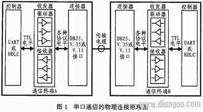
With the further development of communication network technology, more and more serial interfaces in Internet devices (such as routers, switches, gateways, access devices) are designed to support multiple physical interface protocols in the Wide Area Network (Wide Area Network). standard. WAN serial port protocols include RS-232, RS-449, EIA-530, V.35, V.36, and X.21. Figure 1 shows a simple serial communication interface diagram. It can be seen from the figure that the key to realize multi-protocol serial communication is to convert the different transmission modes, balanced, unbalanced and different electrical signals sent by the connector into signals with TTL level that the terminal can recognize and process through the transceiver.
1 Characteristics and problems of traditional multi-protocol communication
1.1 "sub-board" mode
A common implementation in WAN serial applications is to provide a separate daughter board for each physical protocol required. A system that supports the EIA-232, EIA-449, and V.35 protocols typically requires three separate daughter boards and three different connectors. This method requires a sub-board to be configured for each protocol. Therefore, the system needs to manage the PCB sub-board, the transceiver chip, the connector, etc., which wastes resources and complicates the management work.

1.2 universal connector mode
To solve the shortcomings of the "sub-board" method, a motherboard and a universal connector can be used. There are a variety of transceiver chips on a motherboard, which can meet the requirements of multiple serial protocols, and can share some common devices, while reducing the waste of resources. In the configuration, you should pay attention to the problems caused by the small number of pins of the connector. It is better to allocate the pins according to the signal instead of the protocol, that is, assign a common pin to each signal, regardless of its How to define the physical protocol. For EIA-232, EIA-449, EIA-530, V.35 and V.36, the TxD signal can be connected to the same pin of the connector. That is, the SDî—¤a signal is connected to pin 2, and the SDî—¤b signal is connected to pin 14. This pair of pins is then used to describe the transmit signal TxD for all protocols.
This approach also poses a problem in that the I/O lines of all transceivers to the pins of the universal connector must be shared with each other. For example, the transmit data signal line in a V.28 driver chip is connected to the pin 2 of the connector DB-25; at the same time, the transmit data signal line in a V.11 driver chip is connected to the pin 2 of the connector and 14; The transmit data signal line in the V.35 driver chip is also connected to pins 2 and 14 of the connector. Thus, the pin 2 of the universal connector will be connected to three signal lines at the same time, and the pin 14 is connected to two signal lines. Thus, in this configuration, all drivers must have a three-state characteristic to disable unnecessary output. If the transceiver does not have a tri-state feature, a multiplexer is required to select the corresponding output. Another problem that comes with this is that the transceiver generates leakage current when it is disabled. If the V.28 protocol is selected, its theoretical output voltage is 15V. At this time, the driver for the V.11 protocol is disabled, and when it is tri-stated, its output leakage voltage must be low enough to make the driver signal of the V.28 protocol connected to the same connector pin unaffected. If there is a disconnect switch between the transmitter and the receiver, the switch also takes into account the leakage.
1.3 Serial Port DTE/DCE Mode Switching
DTE/DCE switching can be achieved by selecting different connector conversion cables, which minimizes transceiver complexity when implementing DTE/DCE conversion, but has the disadvantage of requiring cable replacement, especially where the device is placed. This is especially true when inconvenience or when DTE/DCE needs to be frequently switched.
If the transmission cable is kept the same, the transceiver can be configured in two sets to support DTE and DCE modes respectively. The driver output of the DTE transceiver is coupled to the receiver input of the DCE transceiver, and the receiver input is coupled to the driver output of the DCE transceiver. In order to control the DTE or DCE mode, the output of the driver or receiver must be tri-stated. When DTE mode is selected, the DCE chip is disabled, its driver and receiver are tri-stated, and vice versa.
Although this method solves the problem of frequent replacement of cables, the design cost is greatly improved due to the use of a set of transceivers, and the size of the serial board is much larger.

2 Multi-protocol serial communication implementation principle
In the traditional design, the corresponding transceiver chip should be selected for a certain protocol. For example, for the RS-232 protocol, the transceiver chip such as DS-1488/DS-1489, MAX232 or SP208 is commonly used; for the RS-449 protocol, it is often used. Transceiver chips such as SN75179B, MAX488, and MAX490. When using RS-232, RS-422, and V.35 protocols simultaneously, multiple transceiver chips are required to support different protocols.
Now, some transceiver manufacturers have developed multi-protocol transceiver chips. Sipex is the first company to produce the RS-232/RS-422 software option protocol chip SP301. This chip combines the electrical characteristics of RS-232 and RS-422 transceivers into a single chip. Among them, SP50X series products can support up to 8 protocol standards. Other manufacturers such as the LTC154x series and LTC284x series chips produced by Linear also have the above functions. Users can choose the right chip according to their needs.
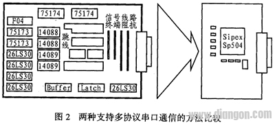
2 is a communication card using a discrete transceiver chip and a multi-protocol serial port communication using a multi-protocol transceiver chip. As can be seen from the figure, the complexity of the former implementation is much larger than the latter, and the specific performance comparison is listed in Table 1.
Table 1 performance comparison of two methods to achieve serial communication
Discrete device board integrated device board power supply voltage +5V, -5V, +12V, -12V+5V required transceiver chip number 121 supported physical layer protocol RS-232, RS-422, RS-449, EIA-530, V .35, V.36RS-232, RS-422, RS-449, RS-485, EIA-530, EIA-530A, V.35, V.36 protocol selection method jumper or switch software or hardware (via internal translation Code) Serial board size requires other hardware support in addition to 15 transceiver chips. Very small power consumption is about 1W, about 100mW ~ 250mWIn addition, multi-protocol transceivers are much easier to handle driver enable control and output leakage current than discrete transceiver chips. When a protocol is selected by software or hardware method, the electrical parameters of the driver and receiver will be adjusted to the appropriate size, and the internal control level of the driver, the input threshold of the receiver, and the impedance of the driver and receiver will be automatically controlled inside the circuit. And the range of common patterns for each physical layer protocol.
In addition, due to the need for V.35 by external network terminals, the connection to the V.35 transceiver is not as simple as other protocols. When using discrete transceiver chips, the V.35 network terminal is often disconnected when selecting other protocol interfaces by using expensive relay switch resistors, or the user is required to change the terminal module once every time a new interface standard is selected, which wastes Resources can complicate interface circuits and are not an ideal implementation. The multi-protocol serial port chip automatically provides the appropriate terminal and on-chip switches to comply with the V.10, V.11, V.28 and V.35 electrical protocols, thus solving the cable termination problem.

3 Multi-protocol communication based on LTC1546/44
In order to illustrate the working principle of the multi-protocol serial chip, Linear's LTC1546/1544 chip is taken as an example for analysis.
3.1 Performance of the LTC1546/LTC1544
The LTC1546 chip is a 3-driver/3 receiver transceiver with the following main features:
â—With software-selectable transceivers supporting RS232, RS449, EIA530, EIA530A, V.35, V.36 and X.21 protocols
â—On-chip cable terminal is available
◠Pin compatible with LTC1543
â—Compatible with LTC1544 to complete the complete DTE or DCE
â—Working at 5V single power supply
â— Small footprint.
The LTC1544 chip is a 4-driver/4 receiver transceiver. Its main features are:
◠Software optional transceiver supports RS232, RS449, EIA530, EIA530A, V.35, V.36 and X.21 protocols
◠Use LTC1344A as software optional cable terminal
◠Complete DTE or DCE port with LTC1543, LTC1544A or LTC1546
â— Works with a single 5V power supply as the LTC1543.
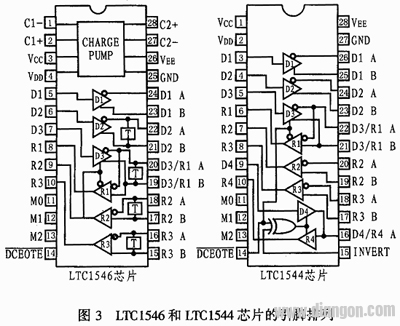
Both chips are packaged in a 28-lead SSOP surface mount package, as shown in Figure 3.
The LTC1546/LTC1544 can form a complete software-selectable DTE or DCE interface for use in data networks, information service units, CSUs, and data service units (DSUs) or data routers. It supports multiple protocols and cable terminations. Provided on-chip, eliminating the need for a separate terminal design. Among them, half of each port of the LTC1546 is used to generate and properly terminate clock and data signals. The LTC1544 is used to generate control signals and local loopback signals (LocalLoop-back, LL). The interface protocol is determined by the mode selection pins M0, M1 and M2. The specific selection method is shown in Table 2.
Table 2 Mode Selection of Communication Protocol
LTC1546 mode name M2M1M0DCE/DTED1D2D3R1R2R3 is not used (default V.11) 0000V.11V.11V.11V.11V.11 RS530A0010V.11V.11ZV.11V.11V.11RS5300100V.11V.11ZV.11V.11V.11X.210110V. 11V.11ZV.11V.11V.11V.351000V.35V.35ZV.35V.35V.35RS449/V.361010V.11V.11ZV.11V.11V.11V.28/RS2321100V.28V.28ZV.28V.28V.28 No Cable 1110ZZZZZZ is not used (default V.11)0001V.11V.11V.11ZV.11V.11RS530A0011V.11V.11V.11ZV.11V.11RS5300101V.11V.11V.11ZV.11V.11X.210111V.11V.11V.11ZV .11V.11B.351001V.35V.35V.35ZV.35V.35RS449/V.361011V.11V.11V.11ZV.11V.11V.28/RS2321101V.28V.28V.28ZV.28V.28 without cable 1111ZZZZZZAs can be seen from Table 2, if the port is set to V.35 mode, the mode selection pin should be M2=1, M1=0, M0=0. At this point, for the control signal, the driver and receiver will operate in V.28 (RS232) mode; for clock and data signals, the driver and receiver will operate in V.35 mode.
Mode selection can be achieved by controlling the circuit or by using a jumper to connect the mode pin to ground or Vcc to control pins M0, M1 and M2, or by inserting an appropriate interface cable into the connector for external selection control. If the latter is used, when the cable is removed, all mode pins are not connected, ie M0=M1=M2=1, and the LTC1546/LTC1544 enters the cableless mode. In this mode, the LTC1546/1544's supply current will drop below 500μA and the LTC1546/LTC1544 driver output will be forced into a high-impedance state. At the same time, the R2 and R3 receivers of the LTC1546 should be terminated with 103Ω, respectively, while the other receivers on the LTC1546 and LTC1544 should be connected to ground through a 30kΩ resistor.
Driver 3/receiver 1 in LTC1546, driver 3/receiver 1 and driver 4/receiver 4 in LTC1544 are enabled via the DCE/DTE pin; the INVERT signal in LTC1544 is enabled for driver 4/receiver 4 Can work. The LTC1546/LTC1544 can be set to DTE or DCE mode by one of two methods: one is to connect the connector with the appropriate polarity to the DTE or DCE end; the other is through the dedicated DTE cable Or a dedicated DCE cable sends a signal to the LTC1546/LTC1544, while using a connector to form a mode of operation that is suitable for both DTE and DCE.
3.2 Typical application
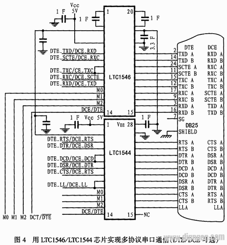
Figure 4 shows a multi-protocol serial communication circuit with a DB-25 connector port and can be set to DTE or DCE mode. The LTC1546/LTC1544 chip is connected to the connector on one side and to the HDLC chip on the other side. The M1, M2, and DCE/DTE pins are connected to the EPLD hardware control circuitry to enable selection of communication protocols and operating modes. The DTE or DCE working mode needs to connect the corresponding cable to ensure correct signal transmission. For example, in DTE mode, the TxD signal is sent to pins 2 and 14 through driver 1 of the LTC1546. In DCE mode, the driver sends the RxD signal to pins 2 and 14.
In Figure 4, the LTC1546 uses an internal capacitive charge pump to meet VDD and VEE. Where VDD is the positive power supply voltage terminal conforming to V.28, the terminal should be connected to a 1F capacitor to ground; VEE is the negative power supply voltage terminal. A voltage multiplier will generate approximately 8V at VDD, while a voltage inverter will produce approximately -7.5V across VEE. The four 1μF capacitors are surface mount tantalum or ceramic capacitors with a minimum capacitance of 3.3μF at the VEE terminal. All capacitors should have a withstand voltage of 16V and should be placed as close as possible to the LTC1546 to reduce EMI interference.
 In V.35 mode, switches S1 and S2 in the LTC1546 will be turned on and a T-type network impedance should be connected to connect the receiver's 30kΩ input impedance in parallel with the T-network termination, but will not significantly affect the total input impedance. Therefore, for the user, the circuit design in this mode is exactly the same as in other modes.
 Since the LTC1546 is a 3-driver/3 receiver transceiver, the LTC1546 is a 4-driver/4 receiver transceiver, so if the RL, LL, and TM signals are used simultaneously, the LTC1546/LTC1544 does not have enough drivers and receivers. Therefore, the LTC1544 can be replaced with the LTC145. The LTC1545 is a 5-drive/5 receiver transceiver that can handle multiple optional control signals such as TM and RL.
All LTC1546/LTC1544 receivers have fail-safe features in all modes. If the receiver inputs are floating or shorted together by a terminating resistor, the receiver's output will always be forced to a logic high.
4 Conclusion
There are many ways to implement multi-protocol serial communication. Different manufacturers provide serial chips with different functions. Designers can choose according to their needs. When designing a complex DTE/DCE mode that supports various physical layer protocols, choosing a single-chip multi-protocol serial transceiver will simplify configuration and design more circuits than using many discrete components. Flexible, convenient and simple.
In the rectifier circuit; the use of diodes in series can increase the back pressure withstand value (usually the sum of the back pressure of all diodes, but it is best to use diodes of the same specification).
In the voltage stabilization circuit; the series connection of the diode is equal to the sum of the voltage stabilization value of the diode. The use of diodes in parallel is theoretically the sum of rated currents, but considering that it is impossible to be absolutely symmetrical, they can only be used below 80% of the total.
TVS transient suppressor diodes work in the same way as regulator diodes, but there are structural differences.The biggest difference is that the PN junction area composed of the general regulator diode is very small, it can withstand the reverse current is small.
Transient Voltage Suppressor,Transient Voltage Suppressor Diode,Series diode
Changzhou Changyuan Electronic Co., Ltd. , https://www.cydiode.com