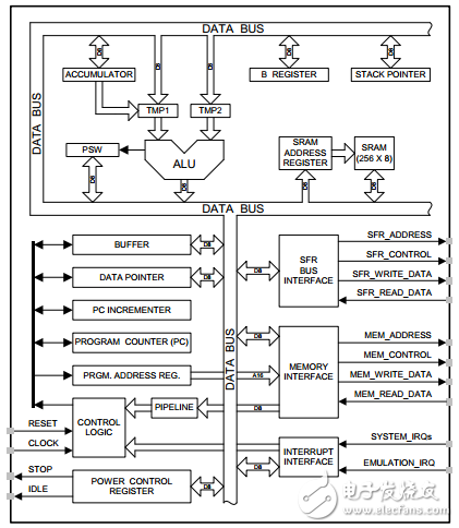
When the 8051 core architecture lost its patent protection in 1998, the well-recognized 8051 core was once again popular. At that time, a variety of new 8051 MCUs continued to enter the market, and some manufacturers continued to adopt the original architecture, while others continued to implement it. Different levels of improvement. The Silicon Labs 8051 architecture is one of these higher performance optimization architectures. It remains compatible with the original kernel code, while modernizing and "RISC-like" the 8051 architecture, resulting in tremendous performance gains. Figure 1 shows the classic three-stage pipeline architecture implemented in the Silicon Labs 8051 core.

Figure 1 - Typical Pipeline Example
The original Intel 8051 core takes 12 clock cycles to execute an instruction; therefore, at 12MHz clock frequency, it can run at up to 1MIPS (million instructions per second). In contrast, the Silicon Labs 8051 core with a 100MHz clock frequency can reach 100MIPS, or it can be said that at about 8 times the clock frequency of the traditional 8051, the Silicon Labs 8051 core with a 100MHz clock speed runs faster than the traditional 8051 core. 100 times.
Silicon Labs implements its 8051 advanced core with a 3-stage pipelined Von-Neuman architecture. The simplicity of the 3-stage pipelined 8-bit machine's explicit instruction decode logic allows the chip to run at 100MHz clock frequency in a 0.35-micron process. Due to the importance of compatibility with the classic 8051 code, the architecture retains a 32-byte register file with four regions, making context switching easier. All other hardware aspects of the Classic 8051 are also reserved for the reasons mentioned above. Figure 2 shows the 8051 core implemented in the next-generation Silicon Labs chip.

Figure 2 - Example of the most advanced 8051 MCU
In order to take full advantage of the capabilities of these new 8051 chips, it is necessary to create a system definition that identifies and utilizes the features provided by this architecture. For example, the 8051 core implements the ability to perform logical operations directly in certain registers or memory locations. This is a very useful feature in almost any control application, whether industrial or otherwise. With the operating frequency of the Silicon Labs 8-bit chip, these operations can be performed in a single clock cycle. This approach results in excellent control response time, which means that bit-banged bus definitions can operate at a fairly reasonable rate when compared to hardware implementations of the same configuration. For example, a bit-banged full-duplex SPI can be implemented for 12 system clock cycles per bit, supporting bit transfer frequencies greater than 8 MHz at a 100 MHz system clock frequency.
Another 8051 innovation is the addition of controllers for flash memory management with embedded flash, which gives the 8051 the ability to quickly boot and execute code. Of course, the instruction fetch path also satisfies the speed requirements, so advanced features such as prefetch buffers, caches, and branch target buffers are also implemented. Silicon Labs' latest 8-bit MCUs, such as the EFM8UBx family, implement traditional 16-bit wide prefetch buffers to support 50MHz operation.
Given the performance characteristics of these systems, the novel I/O architecture must support multiple peripherals to run simultaneously (or time-sharing). To this end, a priority-based Crossbar architecture is developed to allow any peripheral to access virtually any port in a defined manner. Therefore, it is possible to implement multiple high-speed peripherals in the same system with a large number of I/O pins, and all pins can be controlled by a high-performance CPU.
The 8051 core is an 8-bit machine, which means that the register space is limited to only support 256 registers. It's not enough to have only a high-performance CPU and a lot of peripherals. To overcome the limitations of register space, the concept of a memory page is used to implement multiple 256-byte address space definitions, and the mechanism for page switching is also implemented. In addition, some system registers and critical peripheral registers are accessible on every page.
-------------------------------------------------- --------
This article is selected from the "Intelligent Hardware Special Issue" in April. More technical hot texts can be downloaded from the special issue page !

For Huawei Oca,Huawei Oca Sheet,Huawei Optical Clear Adhesive Glue,Huawei P60 Oca Sheet Paper
Dongguan Jili Electronic Technology Co., Ltd. , https://www.jlglassoca.com