FPGA-based systems are becoming more and more popular, and many designers love FPGA-based architectures because of the added flexibility of code or improved functionality. But designing a qualified power supply requires many challenges, starting with multiple power rail problems. The FPGA requires at least one voltage to drive the core and one (or more) voltage to drive the I/O bank. However, FPGA-based systems may require more rails to drive double data rate (DDR) memory, transceivers, Ethernet physical layer ICs (PHYs), ADCs, or small microcontrollers. In addition, these voltage rails require a dedicated architecture: sub-1.25V output, monotonic rise, sequencing, and controlled rise time.
While design engineers and semiconductor manufacturers are always working to provide an integrated, easy-to-use alternative, in many cases designers will still leverage existing features to achieve the best solution far beyond traditional datasheet circuits. In this article, we will explore several commercially available multi-output regulators that can be used as a single-chip FPGA power supply and learn how to implement a sub-1.25V output with some existing bandgap regulators.
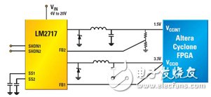
Figure 1 shows a simplified block diagram of a typical application using a monolithic power supply FPGA, such as Altera's Cyclone devices. TI's LM2717 is an integrated dual output switching regulator IC that delivers 2A current (3.2A peak) to the core, 1.5V, 1.5A to the I/O (2.2A peak), 3.3V .

Figure 1. LM2717 dual integrated switch mode power supply for 1.5V core and 3.3VI/O medium power FPGA
The LM2717 is a mid-power, single-chip solution that offers the simplicity and flexibility needed to achieve a compact, 90% efficiency power supply that can meet many digital multitrack system specifications including FPGAs from a variety of Power Supplies. : Conventional power adapters in the 5V, 12V or 4V to 20V range. The LM2717 has an adjustable output and a fixed 3.3V output (common rail) that helps save space and improve output voltage accuracy by installing an internal output voltage setting resistor at the output. The LM2717-ADJ is an improved version of the original LM2717 IC that allows both outputs to be adjustable outputs, which is useful when different I/O voltages are required.
Altera's technical literature on Cyclone and Cyclone II, as well as many other next-generation FPGAs (eg, Xilinx Spartan 3E), shows that these FPGAs do not require any specific ordering of their voltage rails during power up. However, when the system needs to power another FPGA, a single activation pin (SHDN1 & SHDN2) will still appear on the LM2717 in order to turn each output on at a specific time or in a specific order. Similarly, separate soft-start pins (SS1 and SS2) allow the LM2717 to set different rise times for each output voltage to meet the manufacturer specifications for individual FPGAs and other digital cores.
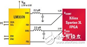
Figure 2 shows a low-power 1.2V, 90nm FPGA (Xilinx Spartan 3L) powered by the LM3370, a dual 600mA per-channel integrated synchronous buck regulator.

Figure 2 LM3370 dual integrated synchronous switching power supply for 1.2V core and 2.5VI/O and VCCAUX low power FPGA
We can adjust the voltage of one channel from 1V to 2V in 50mV step (the ideal value of the core power supply), and program the other channel to adjust the output from 1.8V to 100mV step (I/O power supply ideal value). 3.3V. Each output has a separate active pin, internal soft-start, fast transient response, and power-on reset flag, making this IC a single-chip, minimal external component solution that drives low-power FPGAs and many more The best choice for the rail digital core.
The LM3370 is convenient due to the pre-programmed output voltage and separate activation pins. The on-board I2C-compatible interface allows the user to modify various parameters of the IC, even if it is dynamically modified, for greater flexibility. These parameters include output voltage settings (per channel), output activation (per channel), switch mode selection (automatic PWM-PFM for high efficiency under light load conditions, fixed PWM for fixed frequency operation), spread spectrum characteristics Activate and spread spectrum frequency range selection.
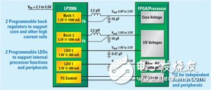
96% high efficiency LP3906 with digitally programmable flexibility
The LP3906 features two programmable buck regulators to support the core and other high current rails; two programmable LDOs to support internal processor functions and peripherals; and an I2C independent control of the LP3906 and peripherals.

Figure 3 LP3906 structure
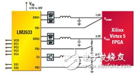
The simplified block diagram shown in Figure 4 shows the implementation of a three-rail, high-power FPGA power supply. In this case, the LM2633 controller supplies 1.0V to the Xilinx Virtex5 core, 3.3V to the I/O, and 2.5V to the VCCAUX. The LM2633 is a three-output IC that is a perfect example of how technology can be used for new applications, breaking through the original application tradition. Two of the three LM2633 outputs use a synchronous rectified buck architecture to provide maximum efficiency to medium to high current loads (5A to 15A per channel), while also integrating an LDO controller for the third low power Output. One of the switched outputs has a voltage range between 0.900 and 2.000, making it the perfect choice for powering digital components. The second switched output range is 1.25V to 6V, enough to power I/O, memory and other loads. For greater accuracy and flexibility, low voltage output programmability is achieved through a 5-bit parallel digital word that can be hardwired or connected to a processor to achieve dynamic voltage regulation when needed.

Figure 4. LM2633 three-switch/linear controller power supply for 1.0V core, 3.3VI/O, and 2.5V VCCAUX high-power FPGAs
Pwm Controller,Home Solar Charge Controller,Pwm Controlador Solar,Wind Solar Charge Controller
GuangZhou HanFong New Energy Technology Co. , Ltd. , https://www.zjgzinverter.com