Many people are confused about the reference plane of the PCB trace. It is often asked: For the inner trace, if the trace side is VCC and the other side is GND, then which is the reference plane?

To figure this out, you must understand the concept of a transmission line. We know that transmission lines must be used to analyze the signal transmission on the PCB to explain the various phenomena that appear in high-speed circuits. The simplest transmission line consists of two basic elements: the signal path and the reference path (also called the return path).
The signal is transmitted in the form of electromagnetic waves on the transmission line. The two basic elements of the transmission line constitute the physical environment for electromagnetic wave transmission. From the perspective of electromagnetic wave transmission, the signal path and the reference path together constitute a special physical structure in which electromagnetic waves are transmitted. From the perspective of the current loop, the signal path carries the signal current and the reference path carries the return current, so the reference path is also called the return path.
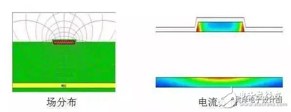
For the surface traces on the PCB, the traces and the underlying planar layers together constitute the physical environment for electromagnetic wave transmission. Here, the network below the trace is what the network properties do not matter, VCC, GND, or even the isolated copper skin without the network, can constitute such an electromagnetic wave transmission environment, the key is that the lower plane is a conductor, which is enough.
The signal path is the surface trace, so the lower plane is the reference path. For this particular structure on the PCB, the reference path appears in the form of a plane, so it is also called the reference plane. From the perspective of the current loop, the reference plane carries the return current of the signal, so it is also called the return plane. The figure below shows the field distribution and current distribution of the surface traces. The role of the reference plane should be clear here: as part of the electromagnetic wave transmission physical environment (from the electromagnetic wave transmission angle), as the current return path (from the current loop angle).

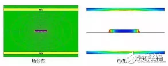
If you understand the above logic, then the reference plane of the inner layer trace is very clear. The trace, the upper plane and the lower plane together constitute the physical environment for electromagnetic wave transmission, so the upper and lower planes are signals. The reference path, which is the reference plane, can clearly see the relationship between the physical environment and the field distribution from the field map below.
From the point of view of the current loop, the current distribution diagram in the figure below also clearly shows the distribution of the return current. If the spacing between the two planes and the traces are approximately equal, the return currents on the two planes are similar. Equal, at this point, the two planes are equally important. From this perspective, it is also well understood that both planes are reference planes. If you still can't understand why both planes are reference planes, don't take a good look at the diagram below. In either respect, the two planes are completely symmetrical. Why are you entangled which is the reference plane? If one is, So why isn't the other?

The most straightforward way to understand the reference plane is to "the physical environment that constitutes the transmission of electromagnetic waves."
Looking at the confused structure, is this condition met?
Can a wide network of isolated copper skins be used?
Of course, the conductor must be in "flat form" to be called the "reference plane", or else the plane is said!
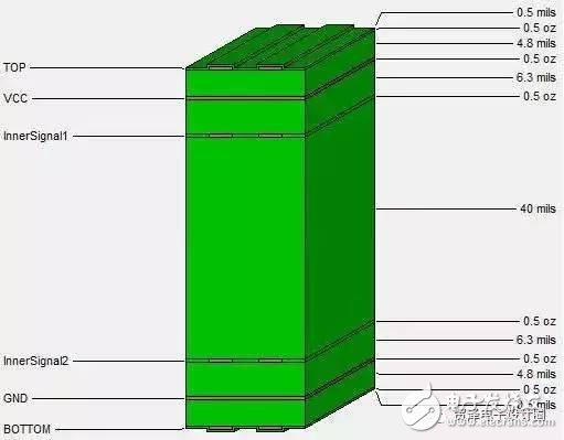
The previous article pointed out that if the spacing between the two planes and the traces are approximately equal (this is common on a dozen layers of boards), then the importance of the two planes for the traces is similar. In actual engineering, we will encounter another situation. One of the two planes is close to the trace, and the other is far away from the trace. For example, a typical 6-layer board configuration, the core thickness of the core is usually Above 1 mm. The following figure is an example of a 6-layer board stack. This is the case for both the inner signal layers InnerSignal1 and InnerSignal2. In this case, the two planes must have different effects on the inner layer traces. Which is the reference plane at this time?

Look at the return current on the plane first, and look at the return current on the VCC plane away from it for InnerSignal2. The figure below shows that the signal current is 10 mA in red and the return current on VCC is about 1.2 mA in blue. The return current on VCC away from InnerSignal2 is very small. When nearly 90% of the return current is returned from the GND plane immediately adjacent to InnerSignal2, the GND plane has a much greater influence on InnerSignal2 than the VCC plane.
Look at the effect of the VCC plane on the inductance of the InnerSignal2 layer trace. The following figure compares the trace impedance with and without the VCC plane. Even if the VCC plane is removed, there is no fatal effect on the trace impedance. The impedance change is less than 1 ohm and the rate of change is less than 2. %. From an engineering point of view, it can be approximated that the InnerSignal2 layer trace reference plane is the closest GND plane to it.
Although it can be approximated, the key is to make sure that the VCC plane far from the InnerSignal 2 layer is not ineffective, but the impact is small. Do not absoluteize the problem at any time, so that there is no harm to beginners. If you always pursue one or the other, black and white, you are likely to walk into a dead end.
In the design of high-speed circuit signal integrity, many problems are like this. What you want to pay attention to is not the question of "have" or "no", but the problem of "multiple" and "less". This way, when dealing with a circuit board that doesn't talk about it, you can have enough cards to prevent it from being tempered and to control it.
NB Personal GPS Trackers,Children GPS Trackers,Kids GPS Trackers,NB Children GPS Tracker,NB kids GPS Tracekrs
eSky wireless Inc , https://www.eskygpsiot.com